
Microcontroller Board for FPGA DSP Radio [160410]
This board is designed to control the FPGA DSP Radio (150177) and other applications. It has a LCD, push buttons, rotary encoders, audio power amp...
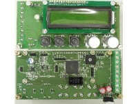
Control board for the FPGA radio (By Daniel Uppström)
This microcontroller board with a 2 x 16 LCD, 3 push buttons, 2 rotary encoders with push button, a small 2 W audio power amplifier, 5 V voltage regulator and more, is specifically designed for a stand-alone control of the FPGA DSP Radio (150177), an alternative to a control by Raspberry Pi. With a Raspberry Pi you’ll need additional hardware like a monitor, keyboard and mouse. This control board is very versatile and can also be used for many other applications.
Control board for the FPGA radio (By Daniel Uppström)
Presented here is a front panel board with display and buttons for the purpose of controlling the FPGA radio. It is based on the Atmel AVR ATmega128A microcontroller.
On the board is also an audio amplifier that can be used to get more power in a speaker than what is available from the audio codec chip on the FPGA board.
The interface used between the control board processor and the FPGA is I2C. This is simple, with few wires, and also adds the possibility to add more nodes to the same bus. With this controller, solder jumper JP1 on the FPGA board shall be left open to select I2C-mode (instead of the optionally selectable UART-mode).
At the time of boot / start-up a few settings are sent to the FPGA that defines the basic operation. Further settings like the frequency, the audio volume and the mode of operation (AM/SSB/CW etc.) can then be controlled by the user.
The controller reads backs status information from the FPGA continuously, from which the received signal strength is indicated, as well as whether the radio is in receive or transmit mode.
Circuit description
The I2C interface for connection to the FPGA board is available at K3.
The SDA and SCL ports are open collector/drain and resistors R2 and R3 pull-up to 5V. This might seem incompatible with the 3.3V used for the FPGA I/O's, but the resistances ensure that only a few milliamps can flow and the body diodes in the FPGA will ensure non-destructive voltages.
Resistors R4, R5 and two ferrite beads L4, L5 attenuate any high frequency noise at the interface.
The processor is programmed by a standard AVR ISP adapter connected at K2.
The crystal X1, together with its loading capacitors C5 and C6, can optionally be mounted but for the current firmware it is sufficient to use the internal RC oscillator in the ATmega128A. This will also likely create less radiation since no clock signals come out of the processor.
The buttons S3, S4 and S5, together with the encoders S1 and S2, form the basic user input interface. Pressing S5 makes coarse frequency steps between frequency bands. Pressing S4 toggles between the modes AM, LSB, USB, CW and CWN (narrow CW filter). S3 is intended as a button for accessing a configuration menu, which is not yet implemented in the firmware.
The rotary encoder S2 is a volume control. By pushing it in while rotating one instead sets a squelch level, such that the audio can be muted below a certain signal strength level.
Rotating S1 tunes the frequency and by pushing it one gets a more coarse resolution.
For serious work, with a lot of tuning up and down, one quickly gets annoyed by a cheap mechanical encoder like S1. It is therefore possible to connect a better optical encoder, with a nice big tune knob, to K1 in order to get the smooth feeling associated to expensive shortwave transceivers. There is then also an acceleration mechanism implemented such that a fast rotation on the frequency dial creates larger steps. The optical encoder ENA1J-B28-L00128L from Bourns is a good alternative that is available at reasonable pricing.
When using the radio for transmission it is often desirable to fine tune the frequency of reception without altering the transmission frequency. This is known as a clarifier and is achieved by connecting a potentiometer at P1 whose voltage is sampled in an ADC channel. When the pot deviates from the middle position an offset is enforced and indicated in the display with a plus or minus sign.
The display, LCD1, is a standard HD44780-compatible 2x16 character LCD. Its contrast is set by potentiometer P2.
LED1 is a RGB type. The idea is to connect te main switch S6 such that the LED is blue when 5V is available but the radio is turned off. When on, there is green light in receive and red in transmit mode. If the squelch is set and the audio is muted, the LED will not light up at all.
The connections at K8 are optional GPIO's to be used for experimentation.
If a voltage supply higher than 7V is available it is possible to mount IC5 to get the needed 5V (IC5 should then be mounted with sufficient heat sinking and insulation). This higher voltage supply can then also be turned on/off by S6 if it is of double-pole type.
K5 and K6 can be used to feed the board with 5V or connect it further to other boards. Note that K5 is before, and K6 after S6. K6 is directly connected to the circuit!
If more audio power is desirable than the 250mW in 8Ohm available from the audio coded of the FPGA board. The differential audio from the FPGA board is fed in to K4 where an opamp circuit (around IC2) makes the signal single-ended. Power amplification is then done in a MAX9711, IC4, to something like 1-2W which should be suitable to get strong audio in a speaker with a proper resonance enclosure.
The processor has then also a means to generate beeps as feedback to the user through a low-pass network between PB7 of IC1 and the input of IC4 (R23/C22/C21/R22). The processor can also mute the audio amp if desirable. PE2 of IC1 is directly connected to the Mute input of IC4.
Firmware
The firmware for the control board is available with open source, accessible from the project web page. By default it is configured for shortwave amateur radio use with the simple radio board presented in a separate article, but it can easily be adopted for other frequency regions etc.
Analog circuit description (from the lab)
The following text is maybe a bit too extended, considering where this part of the circuit is intended for. But, while testing the audio part we encountered some interesting details about distortion produced by ceramic capacitors.
The FPGA DSP Board (150177-1) also contains an audio codec with a class-AB speaker output capable of delivering a maximum output power of 250 mW in an 8 Ω load. Small speakers usually have low efficiency. 80 dB is more or less typical and 250 mW is often too low for a speaker (but enough for a headphone). So we added a small class-AB amplifier on the microcontroller board with more power. We didn’t use a class-D amplifier to avoid additional RF noise. The MAX9711 (IC4) is available in a tiny 4 x 4 mm TQFN package with an exposed pad for heat sinking and has 12 connections (the exposed pad is the thirteenth, connected to ground). Measured output power is close to 2 W in a 4 Ω load with only a single 5 V power supply. This is possible through a differential output stage. The input however is single ended. The speaker driver in the audio codec on the FPGA Board is also differential. It’s best to first convert the differential speaker signal to a single ended signal. Sometimes distortion can be higher if just one output of the differential output stage is used as a single ended source signal. Also, by using a differential signal between the PCBs suppression of noise and interferences is improved. Additionally to suppress any RF frequencies, the converter stage setup around IC2 also acts as a low pass filter. This makes it also very practical should the output of a class-D power amplifier be used as a source. Resistors and capacitors (R11..R16/C9..C12) should have at least 1 % tolerance to get the highest common mode suppression. A 2.5 V reference (IC3, NCP431AVSNT1G, SOT-23-3 package) with a very low output impedance of 0.22 Ω is used to set IC2 to halve the supply voltage. Just a voltage divider (resistors) would otherwise have to be decoupled with a very large capacitor to ensure a high common mode suppression. Here in principle no capacitor is required, and C13 is only for RF decoupling. More than 1 nF for C13 will cause IC3 to become unstable. The opamp used for the differential/single-ended converter is a low power rail-to-rail-input-output type in a small SOT-23-5 package. Despite the low quiescent current of 250 µA Gain-Bandwidth is still 3 MHz. No decoupling capacitors are used at the input (K4) since difference in capacitance, due to tolerance, influences phase relation of the two inputs far beyond the low cutoff frequency and would degrade common mode suppression. This is the case even if 1 % types were to be used, and high capacitance ceramic types usually have a 5 % or higher tolerance. The low cutoff frequency of 133 Hz is determined by C15 at the input of the power amplifier. C15 is a C0G/NP0 size 1206 to keep distortion at low frequencies low. The use of a X7R capacitor would cause a 4 time higher distortion at 100 Hz. A plastic film capacitor would perform even better but the size is impractical (see plot E). C16 is part of an additional low pass filter. Be sure to also use a NP0/C0G capacitor for lower distortion (see Plot F). The use of ceramic capacitors in the signal path as a whole cause the overall distortion to be higher as is specified in the datasheet of the MAX9711. Gain set for the MAX9711 is 2, in the datasheet distortion is specified at a gain of 1. This is the reason why the power amplifier distortion is already twice as high as specified in the datasheet. C9..C12 and C16 define the high cutoff frequency of 8.6 kHz, which is more than enough for voices. More bandwidth is possible by simply decreasing the value of these capacitors. Half the value of each will double the bandwidth. The feedback of the MAX9711 is inverting and so the power amplifier can easily be used as an adder for different input signals. In addition to the audio signal from the FPGA DSP Board a PWM signal from the microcontroller is used to generate an audible feedback when adjusting controls (if implemented in the firmware). A simple low and high pass filter are added for this purpose, R23/C22 and R22/C21 respectively. The power supply of the MAX9711 is decoupled by a polymer aluminum capacitor for low ESR and high ripple current, 18 mΩ and 3.1 A respectively. To improve decoupling of the power amplifier from the main 5 V power supply a 0.22 Ω resistor (R21) is put in series with C20/C18/C19. Of course a little power loss is to be expected. If the output is driven to maximum power in a 4 Ω load (1 kHz/1.8 W/THD+N = 1 %) the ripple on node R21/C20 is 225 mV and 120 mV across the 5 V supply (in our test setup with an external laboratory power supply). To really suppress the ripple on the 5 V supply the capacitance of C20 would have to be much bigger. The impedance of 220 µF at 2 kHz (twice the frequency of the output signal because of the bridge output) is about 0.36 Ω and the ESR of 0.018 Ω is negligible. At this power the voltage drop across R21 is only 0.136 V and amounts to a loss of only 84mW. This is measured using a continuous sine wave and this is a signal not likely to occur in practice and so loss will be a lot less then. A shutdown of IC4 is possible by setting jumper JP1 to OFF if the power amplifier isn’t needed. Current consumption of the MAX9711 is reduced to only 30 µA maximal (0.5 µA typical). Gain of IC4 is set by the feedback resistors R20/R19/R18 and because the output is differential gain is twice as high: Gain IC4 = 2*R20/(R19+R18). Total gain from K4 to LS1 would also be 4 if it weren’t for the high and low pass cutoff frequencies influencing gain at 1 kHz. So total gain is a little less, about 3.64.
Be careful when connecting a speaker. Both output pins carry a signal. Connecting either to ground would mean a short circuit and will probably damage the MAX9711 permanently! If an oscilloscope is used always connect the ground terminal of the probe to ground of the circuit. Never connect it to one of the outputs. To measure the signal across the load use a differential probe or two normal probes.
To connect K4 to the speaker output K2 of the FPGA DSP board twist/braid the three wires. At the FPGA side the ground terminal is not connected.
A project update where everything is put inside an enclosure will be added.
Measurements (+5 V laboratory power supply, IC5 not mounted)
Pmax 8 Ω 1.2 W (THD+N = 1 %)
Pmax 4 Ω 1.8 W (THD+N = 1 %)
Bandwidth 133 Hz – 8.6 kHz
Supply current PCB 0.03 A (no display, no regulator, Pout 0 W)
Supply current PCB 0.64 A (no display, no regulator, Pout 1.8 W/4 Ω)
Gain 1 kHz 3.64 (K4 to LS1)
We also recorded some plots with our Audio Precision Analyzer
Plot A shows amplitude as a function of frequency of differential/single-ended converter IC2 and power amplifier IC4 combined. Low cutoff frequency of 133 Hz is determined a single capacitor. High cutoff frequency of 8.6 kHz is determined by three capacitors and beyond 20 kHz the characteristic is almost equal to a third order low pass filter. Measured at 0.8 W in 8Ω, differential in (IC2) and differential out (IC4).
Plot B shows amplitude as a function of frequency of just the differential/single-ended converter. Cutoff frequency of 10 kHz is a little higher without the power amplifier. Measurements were made at 700 mV differential in and 700 mV single-ended out (IC2).
Plot C shows common mode suppression. Despite the fact that resistors and capacitors in the differential/single-ended converter are ceramic 1 %, 59 dB at the high cut-off frequency is very good and better than expected. The common mode suppression is lowest at the high cutoff frequency because tolerances have the most influence here. Beyond the high cutoff frequency the signals on both inputs are suppressed by the filter characteristic. This measurement was made with a 700 mV common mode input signal.
Plot D shows harmonic distortion plus noise (THD+N) as a function of frequency at an input signal of 550 mV and a bandwidth of 22 kHz. The cyan curve shows THD+N for 1 W in a 4 Ω load. The green curve shows THD+N for 0.5 W in an 8 Ω load. The higher THD+N at the lowest frequencies is caused by the X7R dielectric used for capacitor C15, which defines the low cutoff frequency at 133 Hz. The capacitance varies strongly with voltage across ceramic capacitors. To demonstrate this we replaced the 0603 SMD by a large plastic film (polyester) capacitor and measured THD+N again (plot E).
Plot E shows harmonic distortion plus noise (THD+N) as a function of frequency at an input signal of 550 mV and a bandwidth of 22 kHz The green curve shows THD+N for 1 W in a 4 Ω load. The cyan curve shows THD+N for 0.5 W in an 8 Ω load. With a polyester capacitor for C15 THD+N at the lowest frequencies is now considerably lower compared to plot D where X7R dielectric was used.
Plot F shows harmonic distortion plus noise (THD+N) in a 4 and 8 Ω load with two different dielectrics for C16 and a C0G/NP0 capacitor for C15. THD+N at the lowest frequencies is now almost as low as plot E where a polyester capacitor was used. The two curves with elevated distortion (green and cyan) at 6 kHz are measured with a X7R capacitor for C16. Replacing C16 with a C0G/NP0 (or U2J) will reduce distortion around 6 kHz significantly (magenta and red).
Plot G shows THD+N as a function of output level at a bandwidth of 22 kHz and an 8 Ω load. With increase of amplitude noise has less influence on the THD+N until the maximum output signal is reached at 1.13 W. This is a good example of hard clipping. At a THD+N of 1 and 10 % output power is 1.2 W and 1.53 W respectively.
Plot H shows THD+N as a function of output level at a bandwidth of 22 kHz and a 4 Ω load. With increase of amplitude noise has less influence on the THD+N until the maximum output signal is reached at 1.66 W. This is a good example of hard clipping. At a THD+N of 1 and 10 % output power is 1.8 and 2.3 W respectively.
Bill of materials 160410-1 v1.2
Resistor
R1 = 100 kΩ, 100 mW, 1 %, SMD 0603
R2,R3,R6,R12,R15,R19 = 10 kΩ 100 mW, 1 %, SMD 0603
R4,R5 = 120 Ω, 100 mW, 1 %, SMD 0603
R7 = 15 Ω, 100 mW, 1 %, SMD 0603
R8,R9,R10,R17 = 2.2 kΩ, 100 mW, 1 %, SMD 0603
R11,R14,R18 = 1 kΩ, 100 mW, 1 %, SMD 0603
R13,R16 = 11 kΩ, 100 mW, 1 %, SMD 0603
R20 = 22 kΩ, 100 mW, 1 %, SMD 0603
R21 = 0.22 Ω, 100 mW, 1 %, SMD 0603
R22 = 220 kΩ, 100 mW, 1 %, SMD 0603
R23 = 47 kΩ, 100 mW, 1 %, SMD 0603
P1 = 10 kohm, 200 mW, ± 20%, linear potentiometer, single turn, solder lugs
P2 = 10 kΩ, 150 mW, ± 20%, trimmer single turn, horizontal, through hole
Capacitor
C1,C2,C3,C4,C7,C8,C14,C24,C25 = 100 nF, 25 V, 10 %, SMD 0603, X7R
C5,C6 = 33 pF, 50 V, 5 %, SMD 0603, C0G/NP0 (optional, for now internal oscillator is used)
C9,C10 = 10 nF, 50 V, 1 %, SMD 0603, U2J, C0603X103F5JACTU, Kemet
C11,C12 = 1 nF, 50 V, 1 %, SMD 0603, C0G/NP0, GRM1885C1H102FA01J, Murata
C13,C21,C22 = 1 nF, 25 V, 5 %, SMD 0603, C0G/NP0
C15 = 100 nF, 50 V, 5 %, SMD 1206, C0G/NP0
C16 = 10 nF, 50 V, 5 %, SMD 0603, C0G/NP0
C17,C18,C19 = 1 µF, 16 V, 10 %, SMD 0603, X7R
C20 = 220 µF, 10 V, 20 %, D 6.3 mm max., 0.018 Ω, 3.1 A, spacing 2/2.5mm,
A750EK227M1AAAE018, Kemet
C23,C26 = 10µF, 35V, 20 %, D 6.3 mm max., 0.04 Ω, 2.1 A. lead spacing 2/2.5 mm
870055673001 (WCAP-PTHR Series), Würth Elektronik
Inductor
L1 = 10 µH, 250 mA, 10 %, 0.2 Ω,SMD 1210, NLFV32T-100K-EF, TDK
L2,L3,L4,L5 = Ferrite bead, 1 kΩ @ 100 MHz, 200 mA, 0.6 Ω, SMD 0603, HZ0603B102R-10, Laird Technologies
Semiconductor
D1 = PMEG3050EP, 30 V, 5 A SMD SOD-128
LED1 = LED, RGB, 3 x 20 mA, 5 mm, common cathode, T-1 3/4, 5 mm, L-154A4SURKQBDZGW, Kingbright
IC1 = ATmega128A-AU, SMD TQFP-64
IC2 = TLV314IDBVT, SMD SOT-23-5
IC3 = NCP431AVSNT1G, SMD SOT-23-3
IC4 = MAX9711ETC+, SMD TQFN-12
IC5 = LD1085V50, 5 V, 3 A, TO-220 (3 pins)
Other
K1 = 1x4 header, vertical, pitch 2.54 mm
K2 = 2x3 header, vertical, pitch 2.54 mm
K3,K4,P1,JP1 = 1x3 header, vertical, pitch 2.54 mm
K5,K6,K7 = Terminal block 5.08 mm, 2-way, 630 V
K8 = 1x5 header, vertical, pitch 2.54 mm
JP1 = Shunt jumper, 2.54 mm spacing
S1,S2 = Rotary encoder + push-on switch, incremental, vertical, 0det, 18PPR, EC11E183440C, Alps
S3,S4,S5 = Switch PCB SPST-NO, RA3FTH9, Multimec
S3,S4,S5 = Cap round black height 19 mm, 1S09-19.0, Multimec
S6 = Toggle Switch, DPDT, 28 VDC, 5 A
S6 = Terminal block 5.08 mm, 3-way, 630 V
X1 = Crystal 8 MHz, 18 pF, SMD 5 x 3.2 mm (optional, for now internal oscillator is used) ABM3-8.000MHZ-D2Y-T, Abracon
LCD1 = LCD Module 2 x 16
IC5 = Insulating kit, thermal pad TO-220 + bush TO-220, MK3306/S, Multicomp
IC5 = M3 Screw, Nut, Two Washers, MK3311, Multicomp
LS1 = Mini speaker, 4 W, 4 Ω, e.g. ABS-230-RC, Pro Signal
LS1 = 1x2 header, vertical, pitch 2.54 mm
K1 = 1x4 pin socket, vertical, pitch 2.54 mm
K3,K4,P1 = 1x3 pin socket, vertical, pitch 2.54 mm
K8 = 1x5 pin socket, vertical, pitch 2.54 mm
LS1 = 1x2 pin socket, vertical, pitch 2.54 mm
S1,S2,P1 = Knob, round, 12 mm, shaft 6 mm, e.g. 505.61, Mentor
Optional (very expensive)
128 pulse optical encoder, 5 V, ENA1J-B28-L00128L, Bourns (connect to K1)
1x5 pin socket, vertical, pitch 2.54 mm (encoder has five pins)
Knob, round with indicator notch, shaft diameter 6.35 mm (11K5013-KMNB, Grayhill, it has a hexagon screw and 1/16” allen key is needed, a 1.5 mm allen key is too small)
Misc.
PCB 160410-1 v1.2
Updates from the author