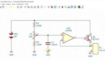
| Elektor engineers love open-source tools. A great example is KiCad, which the Elektor Lab team uses to design schematics and PCBs. Free to u...

More in PCB Design (102)

| Once you know the criteria that matter, how do you use them to obtain the PCB clearance and creepage distances from the EIC 62368 safety sta...

| Electronics manufacturing is rarely easy. Fortunately, the manufacturing process can be simplified with the right tools and services. Felix...

| To determine the clearance and creepage distances between the primary and secondary side of a mains-connected circuit board, safety standard...

| When designing a PCB for a low-voltage circuit that connects to the mains, how much clearance must be used between the mains and the low-vol...

| Need interconnecting pieces of PCBs? Here's a tip: add small ridges along the slots on both pieces that are meant to be put together.
| To avoid footprint mistakes, one of the most common pitfalls of PCB design, board designers tend to rely on footprint libraries provided by...

| Learn how to design PCBs with KiCad EDA. This video takes you from board setup and signal routing via the Footprint Editor and the Design Ru...
| KiCad EDA is a free, open-source schematics capture and printed circuit board (PCB) design tool. After many years of development it has beco...

| The global electronic component shortage poses numerous challenges for a wide range of industries, from automotive to aerospace to medical d...