
Imec and ASML aim for 3nm lithographic process
November 13, 2018
on
on
The research institution Imec and the manufacturer ASML who produce lithography equipment are planning to build a joint laboratory for research into the production of printed nanoscale devices for 3 nm and smaller structures.
They have already successfully collaborated for almost 30 years and are now planning a two-phase five-year program. The first phase is designed to develop and facilitate the take-up of EUV lithography for high volume production. The second phase will investigate the process of next-generation high-numerical-aperture EUV lithography to produce semiconductor structures in the 3 nm range.
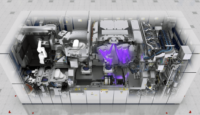
For the first phase, ASML will install the EUV scanner NXE: 3400B in Imecs cleanroom and further refine the current 0.33 NA EUV lithography process. The EUV system operates with a 250 W light source and allows a throughput of more than 125 wafers / hour. The system installed at Imec will be equipped with state-of-the-art alignment and levelling sensors to achieve high throughput with optimum process control and to facilitate adaptation to the latest NXT: 2000i immersion scanner, which will be installed next year.
In the second phase, partners will set up a HighNA-EUV research laboratory to experiment with next-generation EUV lithography using higher Numerical Aperture. The Numerical Aperture (NA) of an optical system is a dimensionless number that characterizes the range of angles over which the system can accept or emit light. Higher NA systems can resolve finer features by condensing light from a wider range of angles.
The next generation EXE: 5000 system will have an NA of 0.55 compared to 0.33 of the current NXE: 3400 system and should be ready by 2021. It aims to meet the challenges of 3 nm exposure systems. This technology is expected to reach the limits of feasibility, considering the silicon lattice spacing is only 0.543 nm.
They have already successfully collaborated for almost 30 years and are now planning a two-phase five-year program. The first phase is designed to develop and facilitate the take-up of EUV lithography for high volume production. The second phase will investigate the process of next-generation high-numerical-aperture EUV lithography to produce semiconductor structures in the 3 nm range.
For the first phase, ASML will install the EUV scanner NXE: 3400B in Imecs cleanroom and further refine the current 0.33 NA EUV lithography process. The EUV system operates with a 250 W light source and allows a throughput of more than 125 wafers / hour. The system installed at Imec will be equipped with state-of-the-art alignment and levelling sensors to achieve high throughput with optimum process control and to facilitate adaptation to the latest NXT: 2000i immersion scanner, which will be installed next year.
In the second phase, partners will set up a HighNA-EUV research laboratory to experiment with next-generation EUV lithography using higher Numerical Aperture. The Numerical Aperture (NA) of an optical system is a dimensionless number that characterizes the range of angles over which the system can accept or emit light. Higher NA systems can resolve finer features by condensing light from a wider range of angles.
The next generation EXE: 5000 system will have an NA of 0.55 compared to 0.33 of the current NXE: 3400 system and should be ready by 2021. It aims to meet the challenges of 3 nm exposure systems. This technology is expected to reach the limits of feasibility, considering the silicon lattice spacing is only 0.543 nm.
Read full article
Hide full article
Discussion (0 comments)