
New microfabrication processes shrink transistors
December 12, 2018
on
on
Researchers from MIT and the University of Colorado have fabricated a 3-D transistor that’s less than half the size of today’s smallest commercial devices. The novel microfabrication process they developed allows them to modify semiconductor material atom by atom.
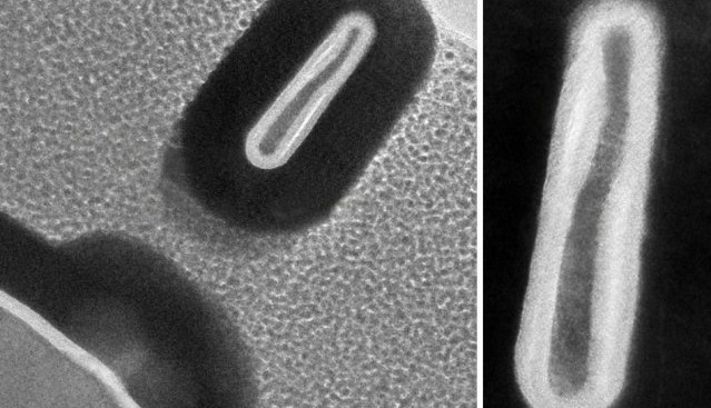
In a paper presented at this week’s IEEE International Electron Devices Meeting, the researchers describe how a recently invented chemical-etching technique, called thermal atomic level etching (thermal ALE), can be modified to enable precision manipulation of semiconductor materials at the atomic level. Using this technique, they were able to fabricate 3-D transistors as narrow as 2.5 nm that outperform their existing commercial counterparts.
Similar atomic-level etching techniques are already in use today but the new process is more precise and yields higher-quality transistors. It employs a common microfabrication tool already in use for depositing atomic layers on materials, meaning the technique can be easily incorporated into existing fabrication processes. The process will allow a higher density of transistors on a computer chip with improved electrical characteristics.
Microfabrication uses deposition (growing film on a substrate) and etching (engraving patterns on the surface) to form transistors. The substrate surface is exposed to light using photomasks to define the outline and structure the transistor. The material exposed to light is then etched away while the pattern under the photomask remains.
These state-of-the-art microfabrication techniques are known as atomic layer deposition (ALD) and atomic layer etching (ALE). In ALD, two chemicals are deposited onto the substrate surface and react with one another in a vacuum reactor to form a film of desired thickness, one atomic layer at a time.
Traditional ALE techniques use plasma with highly energetic ions to strip away individual atoms on the material’s surface. This process causes some degree of surface damage and exposes the material to air, where oxidization causes additional defects and degrades transistor performance.
The University of Colorado’s thermal ALE process closely resembles ALD and relies on a chemical reaction called ‘ligand exchange’. In this process, an ion in one compound called a ligand — which binds to metal atoms — gets replaced by a ligand in a different compound. When the chemicals are purged the reaction causes the replacement ligands to strip away individual atoms from the surface. So far this technique had only been used to etch oxides.
The researchers were able to modify thermal ALE to work on a semiconductor material, using the same reactor used for ALD. They used an alloyed semiconductor material, called indium gallium arsenide (or InGaAs) which is increasingly gaining favour as a faster, more efficient alternative to silicon for chip fabrication.
The researchers exposed the material to hydrogen fluoride — the compound used for the original thermal ALE process — to form an atomic layer of metal fluoride on the surface. Then, they poured in an organic compound called dimethylaluminum chloride (DMAC). The ligand-exchange process occurs on the metal fluoride layer. When the DMAC is purged, individual atoms are removed.
This technique is repeated over hundreds of cycles. In a separate reactor, the transistor’s gate terminal is deposited. Researchers are able to skim away 0.02 nm slices from the material’s surface, giving super high accuracy and allowing careful control of the process. The process is similar to ALD, so thermal ALE can be integrated into the same reactor working on deposition, making it compatible with existing industrial methods.
The technique has been used to fabricate FinFETs devices. Their space-saving vertical fin configuration allows anywhere from 7 to 30 billion transistors to be squeezed onto a single chip. As of this year, Apple, Qualcomm, and other tech companies are using 7 nm FinFETs.
Most of the researchers’ FinFETs are less than 5 nm wide — a desired threshold across industry — and roughly 220 nm high. The fabrication technique also limits defects produced by exposure to oxygen that would otherwise degrade transistor characteristics. The resulting transistor transconductance is about 60 percent better than traditional FinFETs and offers lower operational power consumption.
Read full article
Hide full article
Discussion (0 comments)