Compound memory cell (shown at the bottom in this picture). Image: lancaster.ac.uk
Researchers at the University of Lancaster have developed a new design of nonvolatile memory that can store data using only 1% of the power required by a DRAM and just 0.1% of that drawn by flash memory. The structure was fabricated using 20 nm process...
Researchers at the University of Lancaster have developed a new design of nonvolatile memory that can store data using only 1% of the power required by a DRAM and just 0.1% of that drawn by flash memory. The structure was fabricated using 20 nm process.
According to senior physicist Manus Hayne, the intrinsic memory retention time is predicted to be in excess of the age of the universe. More importantly, writing data requires only one-hundredth of the energy of DRAM or one-thousandth of the power of flash memory. The data is stored as a charge on a floating gate as it is with flash memory but where flash memory uses a layer of oxide for insulation the new memory design relies on the conduction-band offsets in the so-called 6.1-Å family of semiconductors. Here InAs (indium arsenide), GaSb (gallium antimonide) and AlSb (aluminum antimonide) heterostructures are used which offer special electronic properties. The memory cell uses a layered structure. The red balls represent charge. Image: lancaster.ac.uk
A layered structure
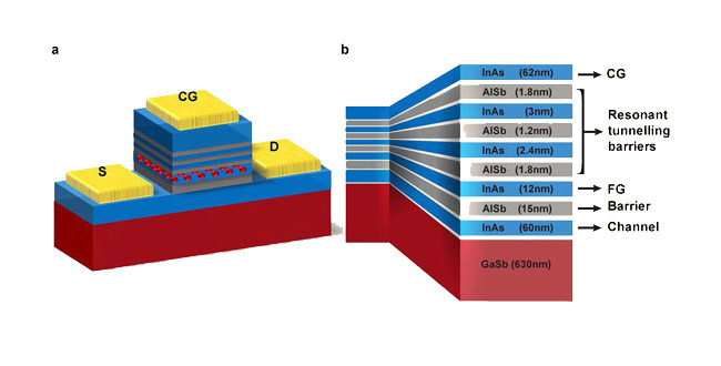
The device underlying the memory cell structure is more like a High-Electron Mobility Transistor (HEMT) than a MOSFET. The intrinsic InAs floating gate is insulated from the InAs channel by a 15-nm AlSb layer, while double InAs quantum wells (QWs) with triple AlSb layers serve as a resonant-tunnelling barrier between the floating gate and the n-doped InAs control gate. Another AlSb layer separates the floating gate from the underlying n-InAs channel - all located on a p-GaSb layer which separates the transistor from the substrate.
An article describing the structure is published in scientific journal Nature with the title ‘Room-temperature operation of low-voltage, non-volatile, compound-semiconductor memory cells’. It describes the use of the conduction band arrangement of AlSb/InAs for charge retention and the formation of a resonance tunnel barrier. The electrons stored in the InAs floating gate are isolated by the abnormally large conduction band discontinuity of AlSb, resulting in a theoretical, thermally activated storage time of an incredible hundred billion years (at room temperature).
Its characteristics
The memory cell was first modeled and then built as a 10 x 10μm (gate dimension) proof-of-concept chip, operating with a bias voltage of ≤2.6V — an order of magnitude less than that required to operate a flash memory cell.
The switching energy in this arrangement resulted in an estimate of 10-17J for the 20nm structure — much less than a DRAM or flash memory cell. A clear differentiation between the ‘0’ and ‘1’ states is maintained throughout a series of erase-read-write-read operations although an upward drift in IS-D was reported as the number of operations increases. This is thought to be a result of charge transfer asymmetry in the write-erase process and reducing the write/erase voltage was enough to prevent the drift.
It is hoped that a new ultra-low energy, universal memory can be built using this technology for use with future mobile smart-devices and IoT endpoint devices.
Read full article
Hide full article
Add a rating to this article
★★★★★
★★★★★
Page 1 / 1
Login
No account yet?Register for free!
Forgot password?
Please enter your email address. Instructions for resetting the password will be emailed to you now.


Discussion (0 comments)