
The Lattice Wearable Dev Platform
December 02, 2015
on
on
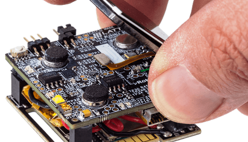
Lattice Semiconductor Corp has announced a development platform for use to design low-power wearable devices. Based on the iCE40 Ultra FPGA, it features a large number of sensors and peripherals making it a good basis to develop a wide range of wearable devices.
The iCE40 Ultra FPGA supports a low power standby mode for always-on functionality, making it a good choice for consumer wearables that need to operate for days between charges.
Key features of the iCE40 Ultra Wearable Dev Platform:
• Wearable watch form factor 1.50“ x 1.57“ x 0.87“ with wrist strap
• iCE40 Ultra (iCE5LP-4K-SWG36) in a 36-ball WLCSP package
• MachXO2 (LCMXO2-2000ZE-1UWG49) in a 49-ball WLCSP package
• LG 1.54” 240 x 240 Single Lane MIPI DSI Display
• Bluetooth Low-Energy Module
• Sensors: Heart-rate/SpO2, skin temperature, pressure and accelerometer/Gyro
• 2 user LEDs, RGB LEDs, High-current White LED and High-current IR LED
• Stereo MEMs PDM Microphones
• 32 Mb Quad SPI-flash
• 27 MHz Oscillator
• Power via built-in 3.7 V, 250 mAh Lithium-Polymer Battery or mini-USB cable
• FTDI 2232HQ USB device allows programming of FPGA and Flash and UART interface to a PC
Included with the platform is a detailed user guide and several demos to demonstrate example applications such as parallel RGB to MIPI DSI bridging, health monitor, pedometer, IR transmitter or flashlight. A reference Android APK file is available to enable smartphone interface over Bluetooth. The iCE40 Ultra Wearable Development Platform is available now direct from Lattice at a retail price of $270.
Read full article
Hide full article
Discussion (0 comments)