Computer chips are approaching the maximum possible density of transistors on a chip - at least in two dimensions. Now researchers at the University of Michigan have stacked a second layer of transistors on top of the first.
Computer chips are approaching the maximum possible density of transistors on a chip — at least in two dimensions. Now researchers at the University of Michigan have stacked a second layer of transistors on top of the first.
The researchers also believe that this process eliminates the need for a second chip to convert between high (peripherals) and low voltage signals (cores).
Moore's Law
Moore's Law states that the transistor density doubles about every two years. As silicon transistors have become smaller and smaller, their operating voltages have also become lower. But higher voltages would damage the tiny transistors. Therefore, the internal structures of modern CPUs are not directly compatible with the levels of the peripherals. However, with the help of 3D arrangements, it is possible to integrate transistors for different levels, because the second layer of transistors can handle higher voltages, thus enabling a more compact chip.
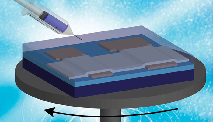
The researchers used a different type of semiconductor for the second layer with amorphous metal oxide. To avoid damaging the lower silicon layer, it was wetted with a solution containing zinc and tin. A uniform covering layer was generated by centrifugal force. Then the chip was dried.
This was repeated until the zinc-tin layer had reached a thickness of about 75 nm. During a final drying process, the metals reacted with the oxygen in the air, and the result was a layer of zinc-tin oxide. This layer was used to make thin-film transistors that could tolerate higher voltages than the underlying silicon.
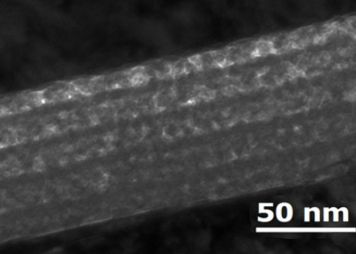
Zinc-tin-oxide semiconductors under the electron microscope - five grey layers.
Picture: Youngbae Son and Rose Anderson, Peterson Lab / UM.
Now the two layers had to be connected. For this purpose, vertical thin-film diodes and Schottky transistors were implemented in the zinc-tin-oxide layer. These components are used for level adjustment of the two layers. This process paves the way to ICs that are integrated higher than Moore's Law allows.
Read full article
Hide full article
Add a rating to this article
★★★★★
★★★★★
Page 1 / 1
Login
No account yet?Register for free!
Forgot password?
Please enter your email address. Instructions for resetting the password will be emailed to you now.

Discussion (0 comments)