
Lattice Announce tiny Footprint MachX03 FPGA
on
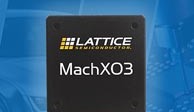
Lattice Semiconductor has announced the release of their MachX03 family of FPGAs. While not the fastest or largest FPGA on the market the emphasis is on affordability, low power consumption and small (2.5 x 2.5 mm) footprint. The chip uses a 40 nm process (compared to 65 nm of its existing MachX02 family) and supports a respectable 3.125 Gbps SERDES transceiver.
The chip is capable of 150 MHz fabric speed and is quoted as consuming microwatts in static and milliwatts in active mode.
The low-density FPGA offers devices ranging from 640 to 22 K logic cells with up to 540 I/Os, unit costs are in the region of 1 cent per I/O. Other features of the device include instant-on capability, on-chip regulators to simplify power supply design and multi-time programmability (with hot-swap I/O facility) to give trouble free in-field upgrades.
Discussion (0 comments)