
KiCad 7: A Look at the Key Features
on
Since its appearance in the early 1990s, KiCad has evolved into a viable alternative to commercial EDA solutions. Ready to try the seventh version? Take a look at KiCad 7 and it features.
Editor's note (July 2024): KiCad 8 has been released, bringing a host of new features and improvements to the popular EDA tool. Elektor engineers are diving into this latest version to explore its capabilities and how it can enhance design workflows. With that said, we know that many of you are still working with KiCad 7, and the information in this article remains relevant for those who haven't transitioned. Whether you're planning to upgrade soon or sticking with KiCad 7 for now, the insights and tips shared here will continue to be valuable. Stay tuned for more updates and guides on KiCad 8 as we dive deeper into its new features! Visit our Circuits & Circuit Design page for updates.
KiCad 7: An Introduction
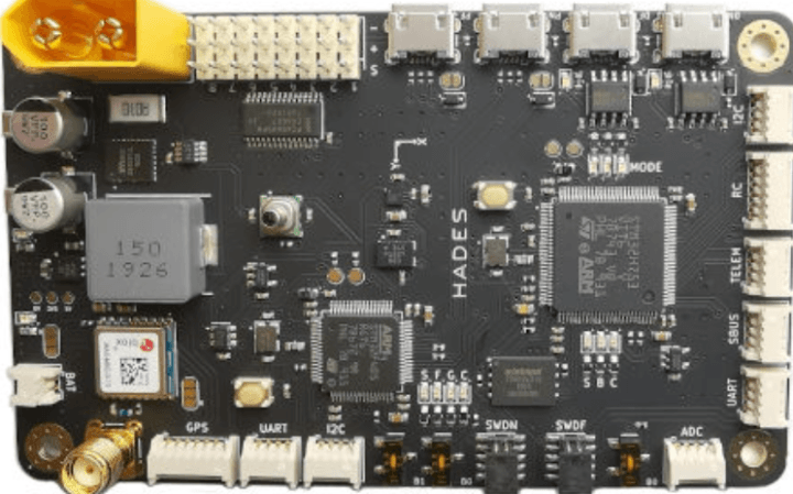
If you are reading this article, chances are you are familiar with (or at least have heard of) KiCad. Just in case you haven’t, KiCad is a popular open-source electronics design automation (EDA) software suite for creating printed circuit board (PCB) designs. It provides tools for schematic capture, PCB layout, and 3D visualization of the board. KiCad supports many standard file formats, making it compatible with a wide range of other EDA tools. It is available for Windows, macOS, and Linux platforms. You can use KiCad to create printed circuit boards, such as the board in Figure 1. This is the main board of the HADES UAV Flight Control System, designed by Philip Salmony using KiCad (GitHub repository).
Since KiCad first appeared in the PCB CAD world in 1992, it has gone through seven major versions, and it has evolved into a serious alternative to commercial products. I have been using KiCad almost daily since Version 4, when I published the first edition of the book, KiCad Like a Pro.
KiCad 7 was introduced by the KiCad team in early 2023. It represents the next step of evolution for KiCad, with several incremental improvements and additions over KiCad 6. Wayne Stambaugh and Jon Evans, the lead developers for KiCad, presented the changes in KiCad 7 in a detailed blog post on the KiCad website.
KiCad 7 changes are “evolutionary,” not “revolutionary” as with KiCad 6. The KiCad 7 user interface is very similar to KiCad 6. The schematic and layout editors look unchanged without detailed examination. Most dialog boxes also seem unchanged, except for some widgets (such as text boxes and radio buttons) being moved around. I expect that most people who are familiar with KiCad 6 will be able to find their way around the KiCad 7 user interface without any trouble.
In this article, I will present the three most important features of KiCad 7: the Plugin and Content Manager, the PCB editor, and improved part modelling. If you are keen to learn more about the new features and changes in KiCad, check out Wayne’s and Jon’s blog posts about versions 7.0.0, 7.0.1, and 7.0.2. Releases 7.0.1 and 7.0.2 contain mostly bug fixes and refinements.
To follow along with the instructions and demonstration, use the latest available version of KiCad 7. If you don’t have KiCad installed, get it from the KiCad website.
Plugin and Content Manager: Better than Ever
KiCad’s functionality can be extended through the plugin system. In KiCad 7, the plugin system, which was introduced in KiCad 6, has reached maturity. Not only is it much more usable than it was in previous versions, but the number of high-quality plugins that are available through it has increased sharply. It is now likely that you will be able to find a plugin for the functionality you want.
In KiCad 7, the Plugin and Content Manager (PCM) automatically checks for updates each time KiCad starts. If it finds updates, it will prompt the user for permission to update the plugin packages.
Here are some examples of useful plugins:
- Interactive Html Bom: An interactive bill of materials (BOM) editor and generator.
- pcb-action-tools: A multi-tool for the layout editor that provides several ancillary functions, such as snapping footprint to the grid and moving drawings to a different layers.
- KiKit: A tool that automates various KiCad tasks, such as penalization, making 3D-printed solder stencils, working with multi-board projects, and more.
- Round Tracks: A plugin that makes it possible to create tracks with smooth and rounded corners.
- Quick-order buttons for various manufacturers, such as PCBWay and NextPCB.
- And, of course, Freerouting, a plugin that offers automatic routing.
To install and manage plugins, you will use the Plugin and Content Manager. This tool is accessible via the KiCad project application, and also allows you to install and manage libraries and themes. You can follow the same process to install and manage schematic and footprint libraries and themes.
Installing a Plugin
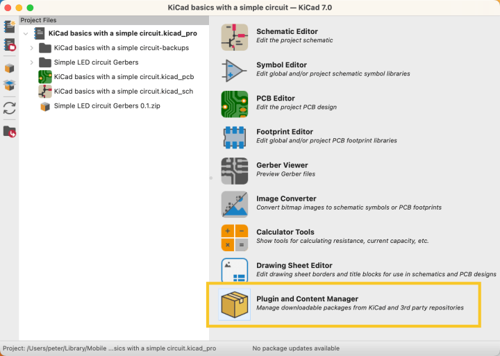
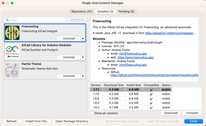
To install a new plugin, start the Plugin and Content Manager tool by clicking on its button in the KiCad project manager window (Figure 2). Plugin and Content Manager contains several widgets as it is designed to fulfil multiple functions.
You can see it in Figure 3.
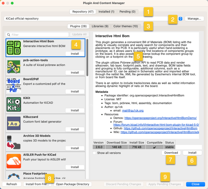
Within the Manager window, you will be able to:
- Select the tab for the type of operation you want to complete (marked “1” in Figure 3): i) Repository allows you to work with content from the repository you have selected in the “repository” drop-down menu (2). ii) Installed allows you to work with content that is already installed. You can update, remove or download a package of the content (both current and earlier versions). iii) Pending shows a list of pending operations.
- Select the repository that you want to work with (2). At the time of writing, I am only aware of the official KiCad repository. As new repositories appear in the future, you will be able to add them to this list using the Manage Repositories window (click on the Manage… button next to the drop-down).
- Select the type of content you want to operate on (3). i) Plugins are packages that implement new functionality. ii) Libraries are packages that provide new symbols, footprints (or both) for your schematics and layouts. iii) Color themes provide pre-designed color themes for the schematic and layout editors.
- No matter which type of content you have selected in (3), the Manager window will show you a list of available content on the left side (4) and further details for the item you have selected on the right side (5).
- You can mark a content package for installation with the Install button (6). A package will not be installed until you click on the Apply Pending Changes button (9).
- You can also download a package by clicking on the Download button (7), and install it at a later time by clicking on the Install from File… button (8).
Let’s install the Interactive Html Bom plugin. You can either click on the Install button in the plugin summary box (4), or the Install button in the plugin details pane (6). An alternative is to download the plugin package (click on Download in the details pane (7) and then Install from File… (8).
When you click on the Install button, the install action is added to the Pending list. You can apply the pending changes by clicking the Apply Pending Changes button (9). You can also see a list of pending changes by clicking on the Pending tab in the header of the Manager window (1).
Managing Content
Once the new content is installed, it will appear in the Installed pane. To see what content has been installed, click on the Installed tab (1). You can see my installed content in Figure 4. From here, you can uninstall, update, or download content.
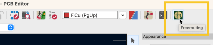
Using an Installed Plugin
The functionality that various plugins bring to your KiCad instance may vary. Some may add one or more buttons to the toolbars, while others may add widgets to configuration and preferences windows. Some plugins may also have additional requirements before you can use them in KiCad. For example, even though I have installed (successfully) Freerouting, I can’t be using until I also ensure that the Java JRE17 is also installed on my computer. In the case of Freerouting, the plugin added a new button in my KiCad instance’s layout editor’s top toolbar (Figure 5). To route a layout automatically using the Freerouting plugin, simply click on the Freerouting button.
PCB Editor: Automatically Complete Trace Route
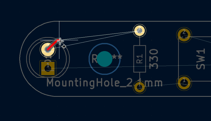
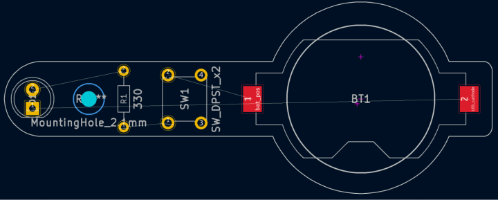
In KiCad 7, routing a PCB is made faster by asking the layout editor to complete the route you have already started drawing. To make this work, use the F shortcut (for “finish”). Let’s look at an example. In Figure 6 you can see the un-routed version of the PCB for one of the projects in the book. Start by switching the active layer to front copper, then type X to activate the Route Tracks tool, and click on pad 2 of the LED footprint to start drawing.
The layout now looks like what you see in Figure 7.
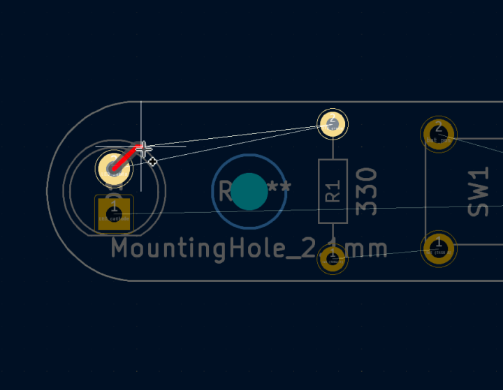
Now, press the F key on your keyboard to get KiCad to finish the operation. The track will finish its route on pad 2 of R1, as in Figure 8.
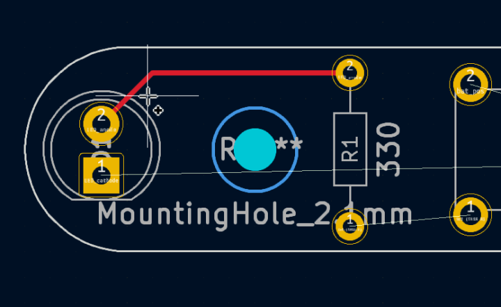
If KiCad is unable to complete an automatic route, it will draw the track as far as it can and then wait for you to take over. This automatic tracerouting feature is a combination between a full autorouter, such as Freerouting, and the interactive router, and is designed to speed up your workflow.
Improved Part Modelling in the Circuit Simulator
In KiCad 6, the SPICE simulator was integrated into the schematic editor. However, only a small number of components were modelled. For almost any practical circuit, you would have to search through online libraries of SPICE component models and import those models into your simulation. I found that to be able to simulate even a simple circuit reliably, you would have to develop serious SPICE expertise. This is far from trivial.
In KiCad 7, however, the situation with the SPICE models is much improved. The simulator now has a graphical model editor that allows you to assign an appropriate model to your schematic components, set their various parameters, and click Start to start the simulation. Let’s look at a simple example.
Say you have this simple circuit, consisting of an LED, a resistor, and a voltage source. You can see the circuit in Figure 9, where (1) is the simulation-ready version of the circuit, and (2) is the original circuit.
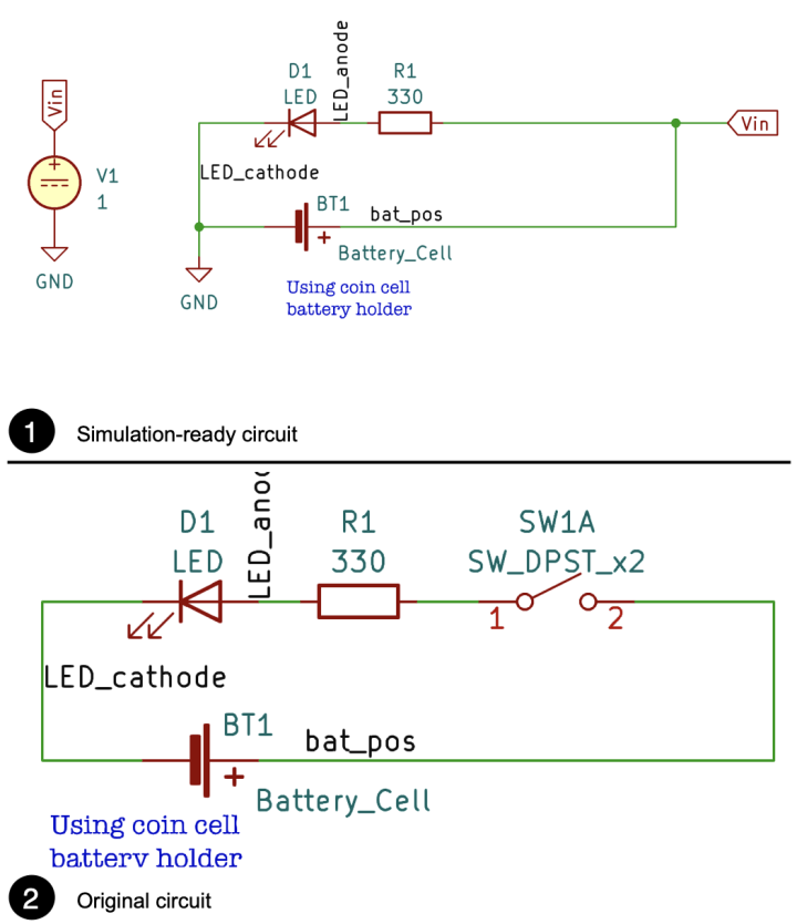
In the simulation version of circuit (1), you will need to assign SPICE models for the active and passive components: the voltage source, the LED, and the resistor.
Let’s drill into the voltage source symbol. Double-click on the voltage source symbol to bring up its properties window, and click on the Simulation Model button to see the SPICE model editor window. Every symbol in KiCad has a SPICE model editor that you can use to set various parameters related to the simulation, including attaching code representing the simulation model of the real-life component.
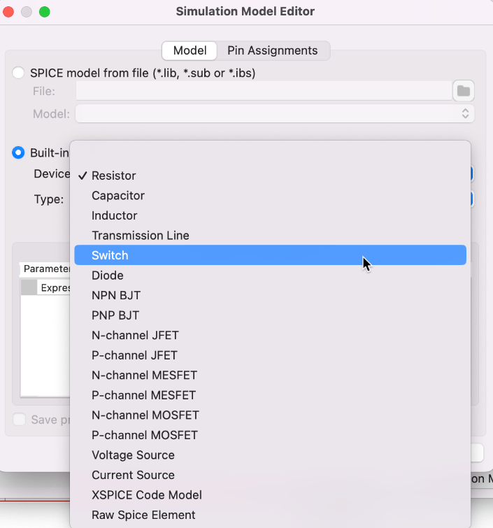
The SPICE model editor window contains two tabs: Model and Pin Assignments. Click on the Model tab. This is where you can configure this symbol (which happens to be a voltage source) for simulation. Explore the various options in the Built-in SPICE model group to see the various devices and types that are available. For example, you can set the source to operate in a pulse, sinusoidal or exponential pattern. Of course, you can set it as a simple DC or AC source. You can also change the device type to something different, such as a transistor, diode, or capacitor.
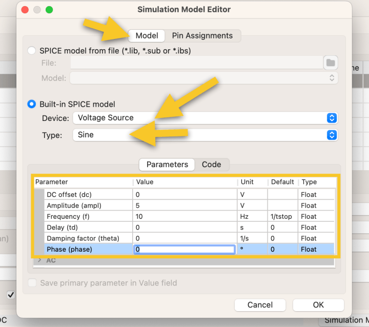
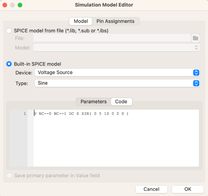
As you can see in Figure 10, I have set the voltage source to produce a sinusoidal (sine) output with 5 V amplitude at 10 Hz. As you define the various parameters, the SPICE code for this symbol is constructed in the background. You can inspect the SPICE model of the symbol in the Code tab (Figure 11 and Figure 12).
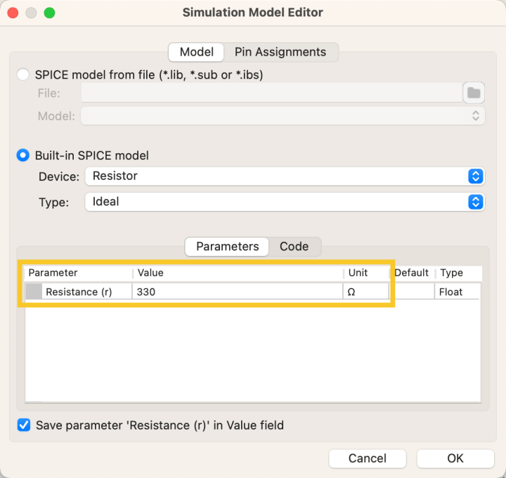
Each model is configurable, and can automatically get values from the schematic symbol properties. For example, see the SPICE model for the resistor in the circuit (Figure 13). The value of the resistor, “330,” was automatically read from the resistor’s value symbol property. Of course, you can still use code to define a SPICE model for a component.
For example, let’s turn to the LED. I used my Google skills to find an appropriate model, which looks like what you see in Listing 1 (source). You can save this model in a text file and import it to the KiCad symbol using the SPICE model editor. I saved the file with the file name led2.model within the directory, Spice Models.
Listing 1: A model for simulation. The lines that start with an asterisk are comments.
.MODEL LED1 D (IS=93.2P RS=42M N=3.73 BV=4 IBV=10U
+ CJO=2.97P VJ=.75 M=.333 TT=4.32U)
*Typ RED,GREEN,YELLOW,AMBER GaAs LED: Vf=2.1V Vr=4V If=40mA trr=3uS
.MODEL LED2 D (IS=93.1P RS=42M N=4.61 BV=4 IBV=10U
+ CJO=2.97P VJ=.75 M=.333 TT=4.32U)
*Typ BLUE SiC LED: Vf=3.4V Vr=5V If=40mA trr=3uS
.MODEL LED3 D (IS=93.1P RS=42M N=7.47 BV=5 IBV=30U
+ CJO=2.97P VJ=.75 M=.333 TT=4.32U)
For the LED symbol, double-click on it to bring up its Properties window, then click on Spice Model. Once the SPICE Model Editor window is up, click on the Model tab, and load the Spice model text file you just created using the File widget under SPICE model from file. Because this spice model file contains three models, use the Model widget to select “LED1” (Figure 14). As you can see in the screenshot, I have used the file method. I saved the model in a text file titled led2.model and used the file browser to find it and select — (1) in the screenshot.
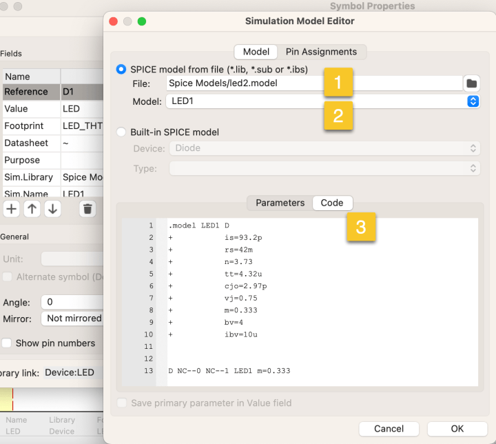
The model file contains three individual models. Each has a unique name: “LED1,” “LED2,” and “LED3”. I selected the model I wanted to use by using the Model drop-down menu (“2” in the screenshot). In the Code tab, you can see the SPICE code that KiCad will use to simulate the LED symbol. The various parameters that you see in the model definitions, such as IBV (Current at Breakdown Voltage), BV (Reverse Breakdown Voltage), and TT (Transit-time), are described in the Ngspice user manual. You can find these values in a component’s datasheet; you can use them in your models.
Click OK and OK to get back to the editor. The circuit schematic is now ready for the simulation. In the next segment, I will show you how to configure the simulator.
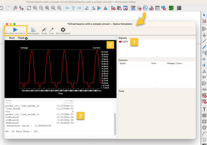
In the schematic editor, open the simulator window (Inspect Simulator) or click the Simulator button in the top toolbar. Click the blue “play” button to run the simulation (Figure 15). My simulation only contains 500 points, so finishing is rapid. In the screenshot, you can see the simulated captured signal (1), the time plot (2), and the results (3). Of course, you can change the simulation.
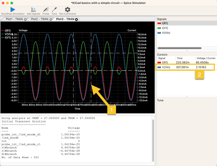
You can create additional plots as needed. With the simulation window active, click File then New Plot. A new tab containing a blank plot will appear in the simulator window. You can add signals and cursors, zoom and pan, and try scenarios with various component values. For example, have a look at Figure 16. This plot shows three signals, I for R1, I for V1 and V for Vin, and two cursors, I for R1 and V for Vin. The cursors allow me to use my mouse and drag the vertical timeline left and right so that I can see the value of the signal at that point in time. I can also use the scroll wheel to zoom in/out and the middle mouse button to pan. The results text window shows the analysis results I can use in my experiment documentation.
Other Upgraded or New KiCad 7 Features
You just saw my favorite three new or updated features in KiCad 7. As you might expect, there’s much more. In addition to the features I have covered, KiCad 7:
- Offers the ability to use custom text fonts, text boxes and graphics primitives in the schematic and PCB editors.
- Allows you to drag and drop files into KiCad apps to them.
- Offers an improved command line interface.
- Allows you to export schematics and layouts to PDF with improved functionality (you can also do this via the command line interface and hence automate export tasks through scripting).
- Contains improvements to the routing engine (with auto-completion of new routes) or unrouting (you can delete an entire route by removing one segment).
- Introduces brand-new Search and Properties panels.
- Offers much improved Pack & Move Footprints.
Grab your copy of KiCad 7 for your operating system now. Download it here!
Editor's Note: This article (230352-01) will appear in Elektor Sep/Oct 2023.
About the Author
Dr. Peter Dalmaris is an educator, electrical engineer, electronics hobbyist, and Maker. Creator of online video courses on DIY electronics and author of several technical books including KiCad Like a Pro (Elektor, 2018) and KiCad 6 Fundamentals and Projects (Elektor, 2022). His company, Tech Explorations, offers a variety of educational courses and bootcamps for electronics hobbyists, STEM students, and STEM teachers. Elektor will publish Dalmaris's latest book, KiCad 7, in mid- or late-2023.
Questions About KiCad 7?
Do you have technical questions or comments about this article? If so, please contact the author at peter@techexplorations.com or the Elektor editorial staff at editor@elektor.com.


Discussion (2 comments)