
System Thermals in Power-Hungry Applications: A Growing Challenge, with Solutions for Improvement
on
Semiconductor-based devices are intended to work within a certain temperature range only. They might malfunction or stop working abruptly if system thermals are not taken care of during the design phase. Let’s discuss heat generation and power losses in the Power Delivery Network, as well as some solutions.
Heat Generation in PCBs
Printed circuit boards (PCB) — the core of any hardware system or electronic device — are engineered to enable the transfer of power and signals from transmitters of power and data to receivers within the circuit. Power losses occur during the electron’s journey within the PCB from one end to another, and heat gets generated. As power losses depend both on the DC resistance and AC impedance of the tracks, so does the heat generated.
Not only the tracks on the PCB but also critical integrated circuits (IC) like power converters, drivers, MOSFETs, IGBTs, and level translators contribute significantly to heat generation. As technology progresses, DSPs, SoCs, and FPGAs are designed to operate in low-power domains to lower power consumption and losses along the Power Delivery Network (PDN). Despite this, these devices still generate considerable heat due to their high frequency of operation and intensive, power-consuming tasks.
With form factors scaling down, thermal management has become one of the most crucial aspects designers face while engineering a PCB. While ensuring the correct functioning and reliability of the circuit across corners is essential, engineers may not get the luxury of using bulky and costly cooling solutions such as heatsinks, fans, or liquid cooling, given cost and space constraints in modern-day products.
Managing System Thermals
Current ICs made of silicon are rated for a maximum junction temperature of 100°C to 150°C. If this temperature is exceeded, the life of the component will be significantly impacted. Inefficient thermal management has the potential to lead to a temperature increase of about 15°C to 20°C, which could reduce component life, in my experience, up to about 50%. For instance, some power-hungry devices, like high-brightness LEDs, convert more than 60% of their consumed power into heat, thus requiring custom, high-performance PCBs to deal with high temperatures and protect against IC damage.
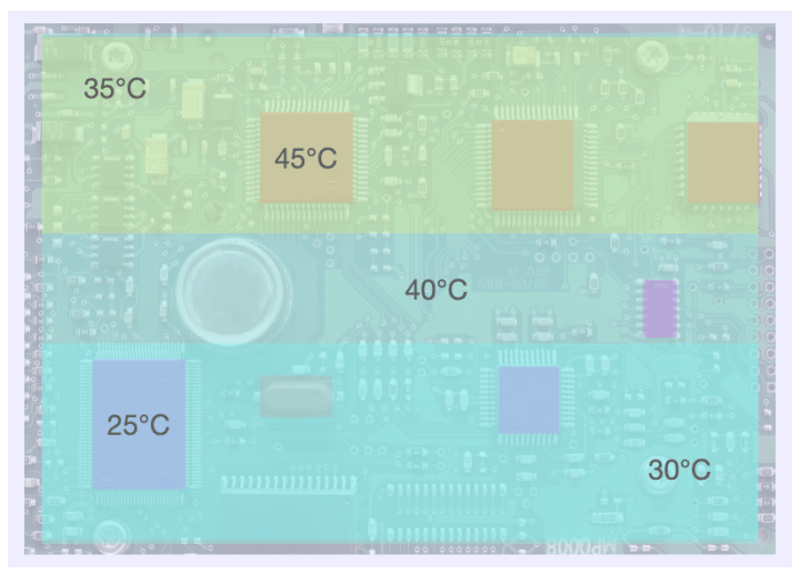
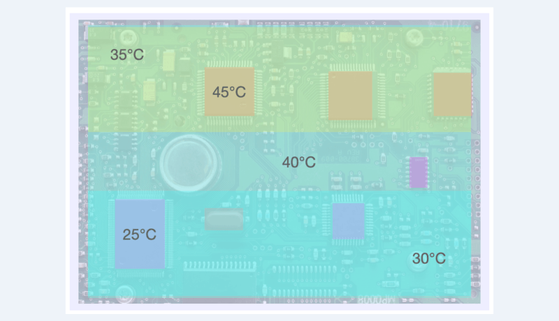
Although modern ICs based on wide bandgap (WBG) semiconductors — such as gallium arsenide (GaN) and silicon carbide (SiC) — are now capable of withstanding much higher temperatures than the conventional Silicon-based devices, the need for accurate thermal management has not been eliminated completely. It is still needed to ensure an even distribution of heat to get rid of thermal hotspots. As an example, Figure 1 shows a thermal image made by an infrared camera: the red colored spots highlight the points of highest heat concentration.
Ways to Improve Thermal Performance
The first step to attaining good thermal performance, even with high-power loads on the PCB, is to figure out the junction temperature TJ and thermal resistance RT of each high-power-consuming IC. The junction temperature of a semiconductor is the temperature at the point where the semiconductor junctions (the internal transistors, diodes, etc.) operate within a component. The maximum allowed temperature for TJ can be figured out in the technical datasheet. Thermal resistance (RT) describes the temperature difference across a thermal path per unit of power dissipated. The thermal pathway refers to the route through which heat is conducted away from heat-generating components to cooler parts of the PCB or external heatsinks. One of the main ways to reduce RT is to minimize the length and resistance of the thermal path by improving thermal conductivity through materials, increasing copper plane areas, or using thermal vias.
These factors concern the PCB layout, which will be engineered to meet these requirements. The growing pace towards the miniaturization of power circuits severely constrains the pad size. Hence, to better manage thermals, the engineer should focus on the following two areas. First, keeping the thermal pathways short, to minimize heat buildup and prevent thermal hotspots. This can be achieved by taking appropriate measures at the PCB design phase, as we’ll see below. Secondly, the materials and substrates used to make the PCB, as well as any other heat-absorbing device around it, shall have the maximum possible thermal conductivity (i.e., the material’s ability to pass heat). Materials exhibiting high thermal conductivity, such as copper, are preferred for components that need to dissipate a lot of heat. This requires careful material selection during the project’s preliminary stages through feasibility studies and proofs of concepts.
PCB Layout
The electronics engineer has various options to limit the thermal path length. A first approach is to achieve uniform heat distribution across the board. For this, increasing the distance between the heat-generating tracks is advisable, This reduces the risk of thermal hot spots. This option is usually constrained by the need to limit the PCB size, sometimes to some extreme extents, as in wearable electronics.
Besides distance, the geometry of the tracks is also a significant contributor. Tracks connecting power components should be shorter and broader. The criteria for track width are derived as a function of the current density and can be obtained from the IPC charts such as the 2221A, which are standards related to PCB design. If tracks used are too small for a given current, they risk overheating and inducing too much voltage drop, leading to degraded performance; if in doubt, using tracks with a broader width is always preferable.
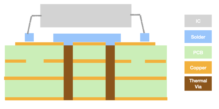
Another frequently used solution is adding thermal vias to the path. Plated vias can be plated to connect different layers together, thus better evacuating heat. Unplated holes can also be used, enabling fresh air circulation. Plated vias are more efficient, as the copper coating allows more heat to transfer. Figure 2 depicts how placing the thermal via right beneath the hot component helps for heat conduction.
Besides thermal vias, another way of removing heat from components is creating large copper polygons in the PCB, thus increasing the available area to disperse heat. The best heat spread is undoubtedly achieved when the top and bottom layers of the PCB are solid ground, where the ability to transfer heat to the ambient air is best, but creating such planes on the internal layers of the PCB helps too.
Finally, copper trace thickness is also an important factor. Using thicker copper for the power tracks and power planes reduces the resistance and impedance of the Power Distribution Network. Using heavier copper layers than usual in power-hungry applications is a good way to attain effective heat dissipation. This allows to increase the PCB’s maximum tolerable current and temperature resistance without incurring failures or degraded operations. While standard PCBs have about 100 µm thick traces, custom PCB can use heavier tracks, up to 2-mm thick in very large motor drives and power electronics, and withstand extremely large currents.
Material Selection and Manufacturing Techniques
Although Flame Retardant Level-4 (FR-4) PCB material is one of the most common, and can help achieve the heat dissipation needs for several kinds of electronic circuits, there are many other use cases where it is essential to utilize materials and substrates with custom electrical properties to address a particular need. Such use cases include radio frequency (RF) applications and small form factor devices like wearable electronics, where it is impossible to use heat sinks or other cooling mechanisms.
In these cases, several parameters help determine whether the material is suitable or not. These include the dielectric constant (DK), the dissipation factor (DF or tan δ), the coefficient of thermal expansion (CTE), the resistivity, as well as the thermal conductivity (k-value). Furthermore, these critical electrical properties of the material should remain stable across different temperature and frequency conditions. This ensures that power losses are minimized under all operating conditions.
Some advanced manufacturing techniques are now being explored across industries, such as Metal Core Printed Circuit Board (MCPCB) and Copper Coin. The MCPCB node integrates a thermally conductive pre-impregnated (prepreg) material between the PCB layers to extract heat from the hot component and redirect it toward the metal planes. On the other hand, the Copper Coin technology consists in incorporating a solid piece of copper under components, to bring heat to the other side of the PCB where it can be dissipated either by a ground plane or an external heat sink. When heat concentration around particular components is an issue, this technology comes in handy, thanks to copper’s high thermal conductivity.
Optimizing Further
Proper PCB design is crucial to managing system thermals. Designers now have various ways to lower the induced heat and improve its dispersion. The main steps to obtain satisfactory results are the choice of materials, manufacturing techniques, and layout. With software tools capable of performing thermal analysis in 3D, designers can do custom simulations based on use cases to understand how heat transfer occurs throughout the circuit and the system.
Comments About System Thermals?
Do you have questions or comments about this article or system thermals? Feel free to contact Elektor at editor@elektor.com.


Discussion (1 comment)