
Versatile Power Supply for Breadboards
on
Breadboard power supplies are useful when no desktop lab power supply is available. Most of the modules on the market are limited to positive output voltages, lower than the input voltage. The project we present here is different. With the help of two integrated circuits from Maxim, a 5-V micro-USB adapter at the input provides up to four adjustable output voltages, three positive ranging from 0.6 V to 20 V and one negative from -1.8 V to -11 V.
Breadboard Power Supply
A breadboard is not only a handy tool for experienced electronics engineers who want to test something quickly, but also for beginners, makers or students taking their first steps in the world of electronics. No soldering is required to build a circuit and changing components or wiring is very easy. Because every circuit needs to be powered in one way or another, we have designed a power supply that can easily be used on a breadboard.
Although a benchtop power supply is the preferred power source when experimenting with electronics or prototyping, this type of lab equipment is not always available. On the other hand, 5 V power adapters with micro-USB plugs are everywhere. We all probably have more of these lying around than needed for powering or charging the devices we own, like mobile phones and other electronic equipment and gadgets. Most of these adapters are short-circuit proof, and combined with the project we present here, you have the perfect, affordable solution for powering circuits on breadboards. Power is limited, but as we all should know: breadboards are not designed for, and definitely not suitable for, high-power circuits.
There are many breadboard power supply PCBs on the market, but unlike this one, most are limited to output voltages lower than the input, and negative or symmetrical outputs are even more rare, if not non-existent. The circuit presented here is a novelty in that respect. It is designed so that you can quickly create a negative or symmetric (e.g., +9 V/-9 V) power supply from your standard 5 V power adapter for, for example, an op-amp circuit. The positive output voltage can even be up to 20 V! But you can also make a low 3.3 V for your microcontroller. It is all adjustable. The breadboard power supply board contains only two integrated circuits and is designed to provide four output voltages: one negative and three positive.
Power Supply Schematic
Figure 1 shows the schematic of the breadboard power supply.
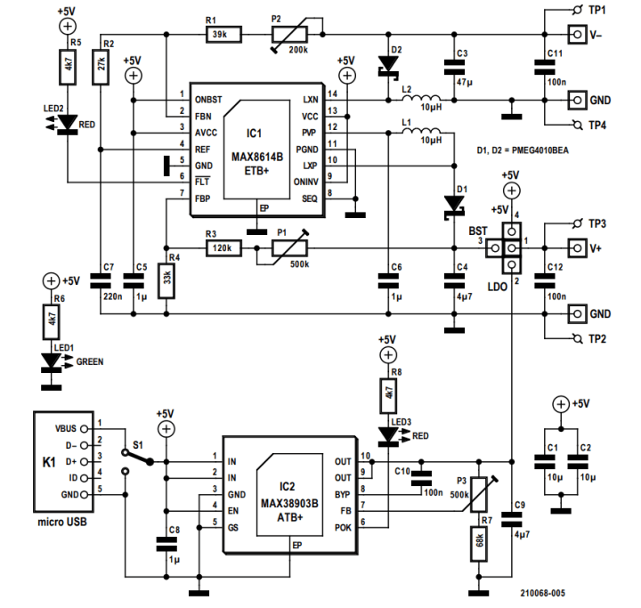
The heart of the circuit is the Maxim MAX8614B.[1] It is equipped with a boost converter that can generate a voltage (VBST) higher than the input voltage and an inverting buck-boost converter that can generate a negative voltage (VINV).
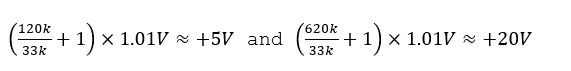
Potentiometer P1 is in the feedback of the positive boost converter, allowing the output voltage to be adjusted between:
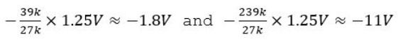
The inverting buck-boost converter also has a potentiometer (P2) in its feedback circuit which allows its output voltage to be adjusted between:
The maximum output power that the converters can deliver is about 2 W for the boost converter and 1 W for the buck-boost converter. This means that for higher output voltages, the maximum output current will be lower. Remember that also the ripple voltage increases with higher loads. It is therefore recommended to place an electrolytic capacitor of a few hundred micro-Farads on the power rails of the breadboard. Pay attention to the polarity of this capacitor and check its voltage rating!
The second integrated circuit in this schematic is the MAX38903 (also from Maxim, see [2]), which is a linear voltage regulator (LDO) that can be adjusted with P3 to an output voltage between:
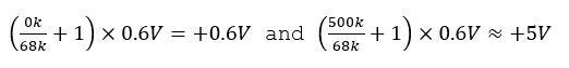
With an LDO, the output voltage cannot be higher than the input voltage. The maximum output voltage will depend on the voltage of the power adapter (5 V here), the losses in the cable/connectors and the drop-out voltage of the MAX38903. In practice this maximum is about 4.5 V. The maximum current this LDO can handle is 1 A. Most adapters can deliver this, but at lower output voltages the power dissipation in the chip will increase significantly:

This dissipation should not exceed 2 W, so 1 A can only be supplied at output voltages higher than 3 V. Fortunately, the MAX38903 is equipped with various protection circuits, so we do not have to worry that our power supply goes up in smoke because the power limits are exceeded. The circuit on the breadboard itself is of course at your own risk.
Assembly
The Gerber files for ordering the PCB are shown in Figure 2.
The DesignSpark design files are available for download at [3].
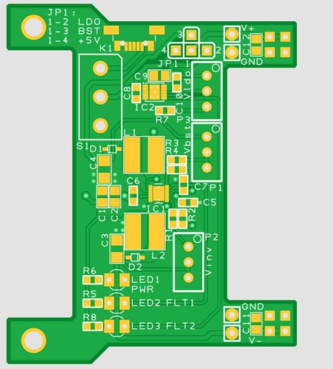
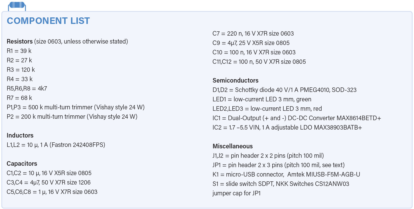
The PCB has been kept as compact as possible, best thing to do is to place the SMD components first, starting with the ICs. Soldering these tiny parts in their TDFN-packages is quite a challenge and building is certainly not recommended for inexperienced makers. There will be soldering wizards who can solder the pads on the sides of the packages with a small iron, but soldering the exposed pads underneath requires a hot-air station or reflow oven. Solder paste is preferred, even though the designer managed to build his prototypes by tinning the pads with normal solder wire, applying extra flux and using a hot-air station for reflowing. A magnifying glass, digital microscope or even a stereo-microscope will be a great help to inspect the solder joints before you proceed with the other components. Soldering the micro-USB connector may seem less challenging but will be a good one to come in third. Next, the surrounding coils, diodes, resistors, and capacitors can be mounted and finally the through-hole components, such as the switch, LEDs and pin headers, that can easily be handled using a normal soldering iron. For JP1, two outer pins of one of both rows of a 3 x 2 pin header are cut off, making it a triangular-shaped, 4-pin jumper configuration.
Usage
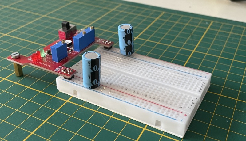
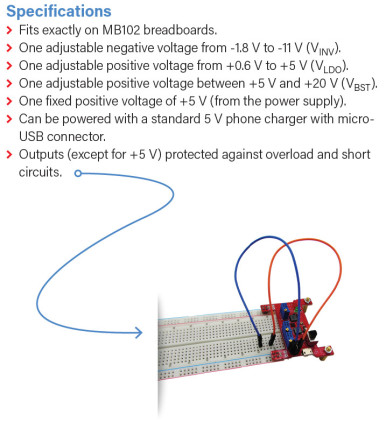
The power supply can be plugged into the breadboard as shown in Figure 3.
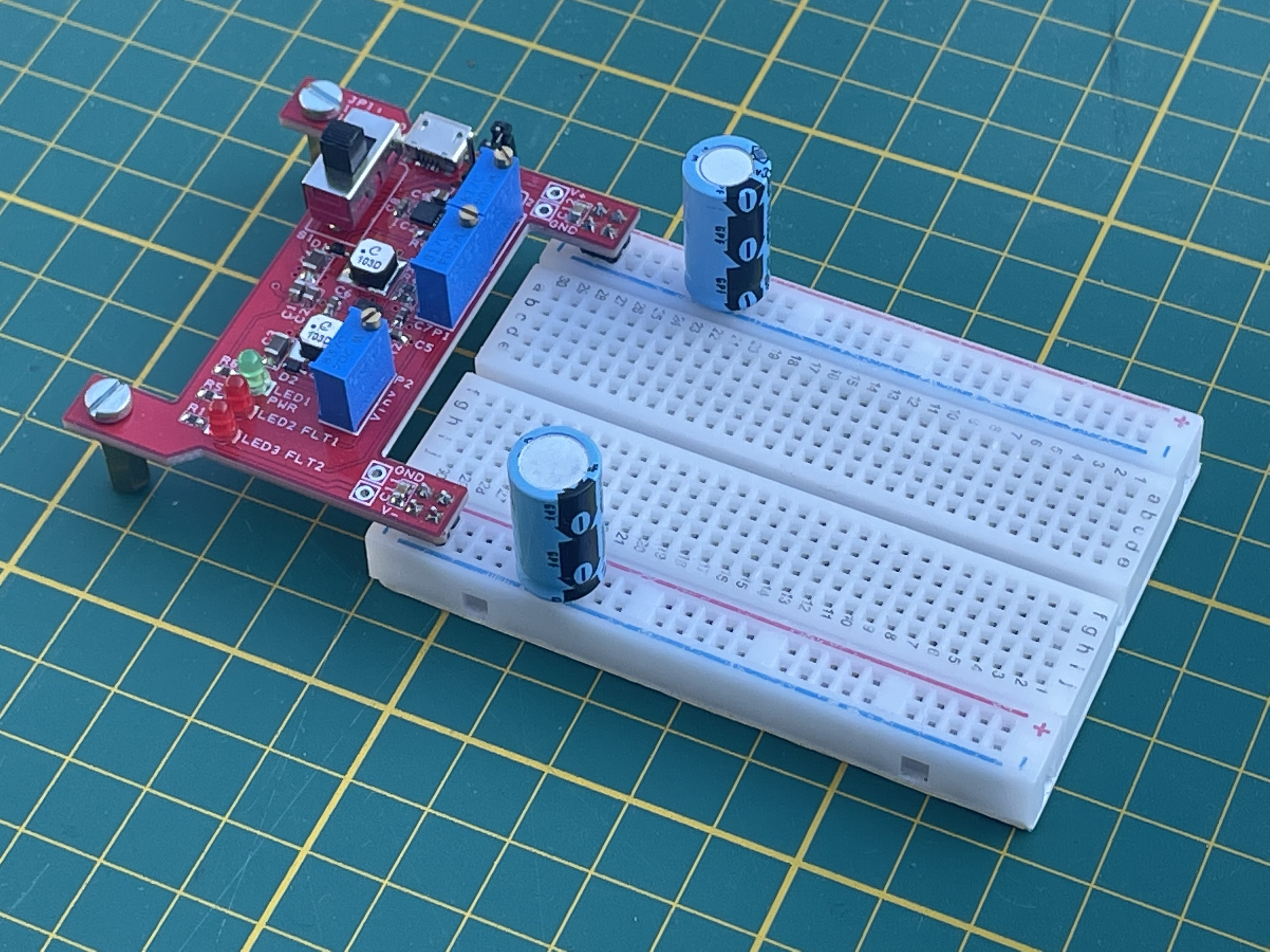
Connectors J1 and J2 are plugged into the horizontal power rails of the breadboard. The top rail is then connected to V+, the bottom one to V- and the two inner power rails to GND (all power supplies of this board share a common GND).
The PCB can be supported on the left side on the lab table using two 12-mm M3 spacers or bolts, two mounting holes are available for this purpose. This improves the mechanical stability of the connection between power supply and breadboard and prevents the board from tipping over when adjusting the output voltages.
Switch S1 can be used to switch the entire power supply on and off. When the power supply is switched on, LED1 lights up green as Power-On indicator.
Since there are three positive supply voltages on the PCB, the user must select which one is connected to the upper supply rail of the breadboard (V+); this can be done with jumper JP1. Place the jumper in position 1-2 for the low adjustable voltage (VLDO), in position 1-3 for the high adjustable voltage (VBST) and in position 1-4 for the fixed +5 V. The jumper positions are also marked in the silk screen on the PCB. The two remaining voltages can still be connected to the circuit on the breadboard using male-to-female jumper wires, as shown in Figure 4.
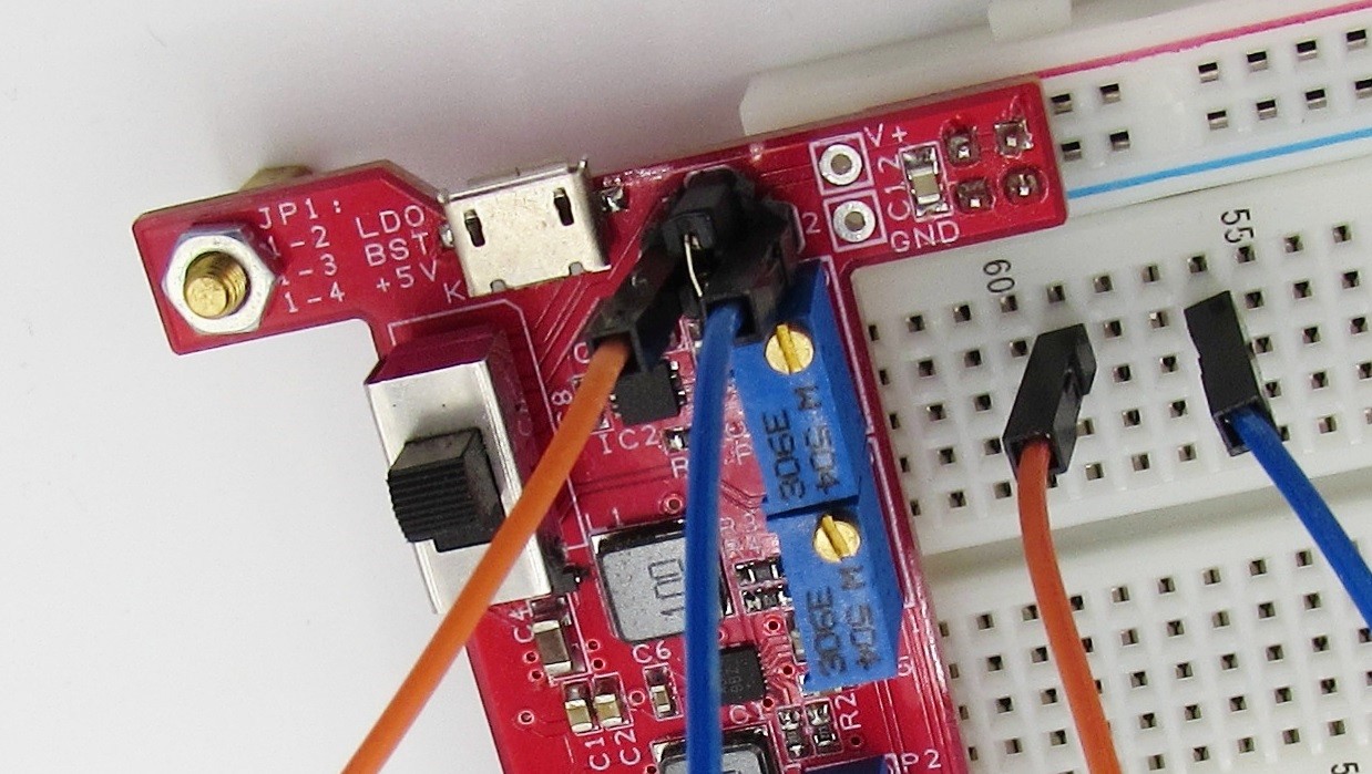
In this picture, the VBST is jumpered to the positive rail, while the orange and blue jumper wires connect the +5 V and VLDO to the breadboard. The negative output voltage VINV is directly connected to the lower supply rail (V-).
The voltages are adjusted by means of multi-turn potentiometers P1 to P3. The silk screen on the PCB shows which trimmer is associated with which output. There are test points for a multimeter to measure V+ (TP3) and V- (TP1) during adjustment, TP2 and TP4 are connected to GND.
There are two red LEDs to indicate an overload or short circuit of one of the power supplies: LED2 (also marked with FLT1 on the PCB) for VBST and/or VINV and LED3 (FLT2) for VLDO. The boost converter and LDO limit the output current at overload and the outputs will be switched off if on-chip thermal limits are exceeded. In both cases the LEDs will be lit. If the buck-boost converter is overloaded, both outputs of IC1 are switched off and LED2 lights. Power-cycling the supply with S1 resets this fault condition, the output voltages will be restored and the red LED will go off again, provided there is no short-circuit, of course. However, there is no overload indication for the fixed +5 V. In this case, we trust that the power supply is short-circuit proof.
Although this project is designed and intended to be used on breadboards, it can of course also be useful as a simple, low-power supply for other applications by connecting wires between the output pins and other electronic (prototyping) circuits. At last, you can put that superfluous 5 V micro-USB adapter to good use on the lab table!
This project can also be found and followed on Elektor Labs website: www.elektormagazine.com/labs/breadboard-power-supply
Discussion (3 comments)