
Linear Voltage Regulator for Fortissimo-100 [220581]
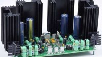
For those who don't want to use a SMPS to power the Fortissimo-100 Power amplifier this is a low-drop high-current discrete symmetrical linear voltage regulator.
A linear low drop voltage regulator designed particularly for the Fortissimo-100 audio power amplifier and a discrete linear alternative for a switched mode power supply. Of coarse other power amplifiers can benefit from a stabilized power supply. The power supply is specifically designed for an output voltage of +/-40 V and 13 A peak currents (15 A peak is possible). The power supply current of a class AB power amplifier at maximum undistorted output power is a half rectified sine wave (with small DC current). The average power supply current of the Fortissmo-100 in a 3 ohm load is 4 A per regulator. 3 ohm is recommended minimum impedance for the amplifier.
The Fortissimo-100 high-end audio power amplifier (https://www.elektormagazine.com/labs/fortissimo-100) works best with a regulated +/-40 V power supply. The classical power supply consisting of a transformer rectifier and large smoothing capacitors is not advised as is explained in the text of the Fortissimo-100. For those who don’t like switched mode power supplies here’s a linear regulator with all through hole components, like the amplifier. Maybe the schematic will give a familiar impression. For the voltage regulator to work without drop-outs the input voltage of the circuit must of course be at least 3 V higher, and in case of possible mains voltage fluctuations even more (most SMPS have a wide AC voltage input range). A linear regulator is less efficient compared to a SMPS and a large transformer must be used, and it must have a higher power rating then without the linear regulator. Most transformers have the same standard secondary voltages. To create +/-40 VDC directly a 2 x30 VAC transformer is the most likely choice. The no-load DC voltage is usually around 42 VDC then, largely depending on regulation of the transformer (the no-load output voltage of a transformer is always a few percent higher) and voltage drop across the bridge rectifier. The next higher standard voltage is 35 VAC and results in approximately 49..50 VDC or more with low power, almost 52 V in a test setup).
At a 8 0hm load (at the amplifier output) the regulator would need only a low smoothing capacitance. Advantage of the larger ripple voltage is a somewhat lower power loss in the regulator. But at lower impedances the ripple should not go beyond the drop-out voltage (43 V at 10 A). In practice a 2 x35 VAC ring core transformer of 300 VA with 20000 µF smoothing capacitance was enough as a power supply for the regulator. Maximum (almost clipping) sine wave power at 20 Hz and 0.1 % THD+N in a 3 Ω load caused only a drop-out peak voltage of 1.8 V (dip at the outputs of the power supply). Mind you, continuous output power is 227 W then in the 3 Ω load and the 300 VA transformer is slightly overloaded! This however was not enough to trip the protection of the amplifier and everything keeps working normally.
To make building of this project easy each of the power transistors in the output stage and their drivers have their own heatsink. So there’s no need to drill 6 holes in one common heatsink.
Schematic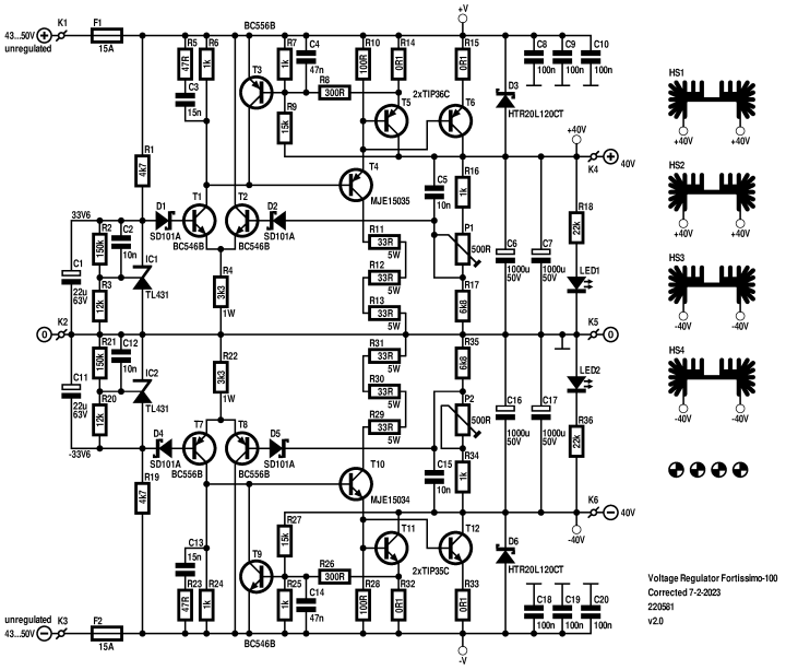
The basis of any voltage regulator is measuring the output voltage and comparing it to a reference voltage and controlling the output stage accordingly. This circuit follows the same concept. A contrast with standard regulators is the much higher (here the secondary) reference voltage, a little over 33 V, close to output voltage of 40 V. The higher the reference voltage, in this case the measured voltage was 33.6 V, the more the internal gain of the simple circuit, a single differential amplifier, can be used to increase ripple rejection of the input voltage and increase output voltage regulation. Simply put, the circuit consists of a reference voltage, a differential amplifier and an output buffer. Additionally a safe operating area protection is added to both regulators. Let’s look at the positive regulator.
The reference voltage
The reference voltage is not created by a Zener diode. Standard ones have high temperature coefficients. Special temperature compensated versions are hard to come by, especially 33 V versions. Instead an adjustable precision shunt voltage reference is used of type LM431. It has a maximum working voltage of 36 V. Its internal reference voltage (so primary reference voltage of the 40 V regulator) is typically 2.495 V. The cathode current through the LM431 is set by resistor R1. If the input voltage is between 43 and 50 V the current is set between 1.9 mA and 3.4 mA and proved to be sufficient to provide a stable 33.9 V reference voltage. The 33.9 V is set by resistors R2 and R3:
VKA = 2.495 * (1 + R2/R3) + IREF * R2
The adjust current IREF of the LM431 is typically 1.8 µA, so the reference voltage is theoretically 33.95 V then. But this is specified at a cathode current of 10 mA. In the prototype this current is lower and so the voltage is slightly lower, 33.55 V was measured. The LM431 is decoupled by C1. C2 improves stability.
The differential amplifier
The differential amplifier is minimalistic and consists of T1 and T2 and R4 as a current source The voltage at the base of T1 is fairly constant and thus the voltage across R3, neglecting the slightly varying voltage across the base emitter of T1 and D1 with temperature. Schottky diodes D1 and D2 limit a possible reverse voltage of the base-emitter voltages of T1 and T2. To reduce the influence of the voltage drop across each diode and not affect the input offset voltage of the differential pair, due to changes in temperature, they are placed next to each other on the PCB and both will have the same temperature. A few millivolts offset or even tens of millivolts, also caused by differences of T1 and T2, have no real effect on the much higher 40 V output voltage. Even an offset change of 30 mV is less than 1 % variance in the output voltage and is inconsequential for the working of the power amplifier. The voltage across collector resistor R6 is used to drive the output stage. R5 and C3, and also C4 and C5, form the frequency compensation to make the regulator stable, even if the SOAR protection T3/R7/R8/R9 is active. Divider R13, P1 and R14 measure the output voltage and are the negative feedback for the differential amplifier. To compensate all tolerances the output voltage range of P1 is approximately 38.6 V to 41.1 V. With the potentiometer in center position the output voltage is very close to 40 V.
The output stage
Although there are transistors that can handle the maximum output current, needed here when a constant 50 V input voltage is applied, two transistors (T5/T6) are chosen to limit power dissipation per transistor, have a larger overload range, lower drop-out voltage and greater safe operating area to reduce the risk of damage to the output stage in case there’s an overload condition or even a short circuit. The larger PNP power transistors are of type TIP36C (NPN TIP35C in the negative regulator) and are available from several manufacturers. PNP transistors are used in the positive regulator to make the minimum voltage drop of the output stage as low as possible, the base currents flow toward ground. The drop-out voltage is the sum of the saturation voltage of the transistors and voltage drop across the emitter resistors. A lower value for the emitter resistors would reduce the drop-out voltage a little but the currents through the two transistors can become too different then. At high collector currents the gain of the transistors is very low and an additional transistor (T4) is needed to buffer the output of the differential stage. To prevent the saturation voltage of T4 increasing the drop-out voltage of the output stage its collector is connected to ground through a series connection of resistors. This limits power dissipation of T4 and only a very small heatsink is required. However, there’s a catch doing this. Should by what ever cause the input voltage fall below the drop-out voltage T4 will conduct permanently and the dissipation in its collector resistor will be quit high: in case of 100 Ω and 40 V input voltage 16 W. But this will or should never occur!. But just in case, to prevent a burn out of this collector resistor three 5 W resistors are used. To save space they are placed upright. An additional advantage of this collector resistor is a limit to the maximum base current of T5 and T6 and forms a simple current limit. The real protection is formed by T3. The output current is measured by the voltage drop across the emitter resistor of T5 by voltage divider R7/R8 and it drives the base of T3. When for instance the current through R14 is about 7 A, total output current is 14 A. Maximum expected output current is a little over 12 A peak (3 Ω load at the output of the amplifier). T3 will start conducting and due to R9 even sooner depending on the voltage across T5. The exact level where T3 starts conducting is temperature depending and will be sooner the higher the temperature. An additional protection. With music this won’t be an issue. D3 protects the output stage in case the input voltage is suddenly disconnected or short circuited. T5 and T6 are each decoupled with a low ESR 1000 µF capacitor. LED1 indicates the presence of the 40 V output voltage. The input is protected by a 15 A fuse. The maximum RMS current must be taken into account and with a maximum half wave sine current the RMS value is Ipeak/2, so 6,5 A. But, at very low frequencies like 16.4 Hz (if you like organ music) the peak current lasts for several milliseconds, and what is the best fuse rating then? To make sure, even in an overload condition, the fuse won’t blow a 15 A fuse is chosen. The voltage drop across the fuse is also lower. If much more power is taken by the amplifier and/or the regulator the primary fuse of the transformer will/must blow. The 15 A fuse will blow should there be a sudden short circuit behind the fuse .
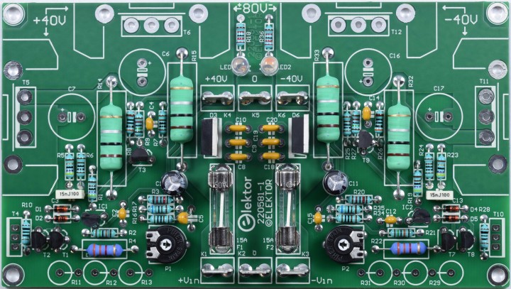
PCB and heatsinks
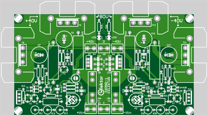
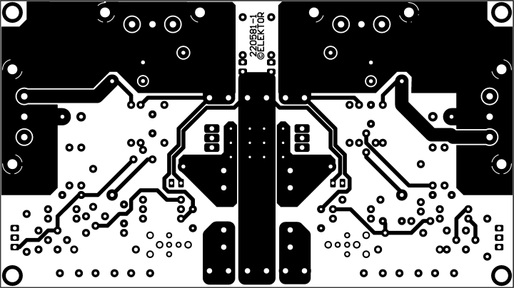
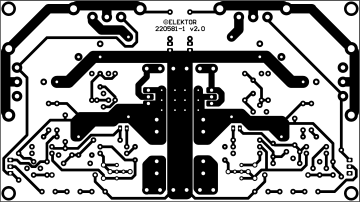
This voltage regulator consists of two independent regulators with a common ground. The reference voltage circuit for the negative output voltage is the same as in the positive regulator, but the resistor R19 that sets the current is connected on the other side of the LM431. The common ground connection of the reference IC1 and IC2 and feedback resistors R17 and R35 are connected to the output ground connector K5 as close as possible. The tracks for the feedback of the output voltages on K4 and K6 are routed alongside these ground tracks to R16 and R34 respectively. To keep the thermal resistance of junction-to-ambient of power transistors T5/T6/T11/T12 as low as possible no insulation is used and the transistor makes contact with their individual heatsinks. This means 80 V is present between the heatsinks of T6 an T12. Never touch any part of the regulator when the input voltage is connected. Disconnect the input voltage when working on the regulator. Also the copper planes underneath the heatsinks are connected to the collectors of the power transistors to minimize resistance to the output. The ground connection from input ground connector K2 to output ground connector K5 is routed on top and bottom using 10 mm wide copper tracks. Also tracks of the 20 A fuse clips of F1 and F2 are routed on both sides. The PCB measures 137.2 x 76.8 mm. With the heatsinks mounted the dimensions of the regulator are 156.8 x 86.7 mm. The heatsinks are purposely placed over the edge of the PCB to maximize airflow. If the PCB is mounted on 10 mm standoffs the total height of the regulator about 76 mm. The footprint of the trimmers allows the use of a simple top adjust single turn trimmer or the use of different type of vertical multiturn trimmers. The input and output connector are vertical spade (faston) connectors for low resistance. The transistors T4 and T10 have their own small heatsinks. Each has two small heatsinks (type FK231SA220, 24 K/W) mounted back to back for lower thermal resistance.
Construction
Start with soldering the lowest parts: small diodes, small resistors, 1 W resistors and the horizontal 5 W resistors.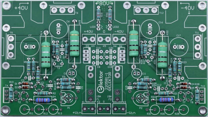
Next trimmers, small capacitors, fuse clips + fuses and faston (spade) connectors. The footprint for the trimmers also permits various types of vertical multiturn trimmers to be used.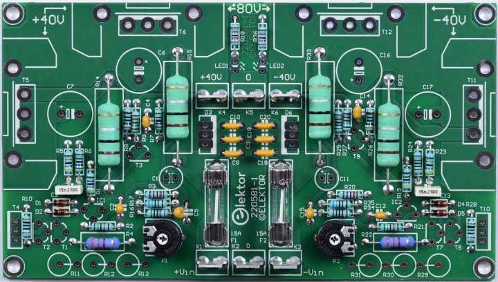
Next small transistors, IC1 and IC2, small electrolytic capacitors, LEDs and D3 and D6.
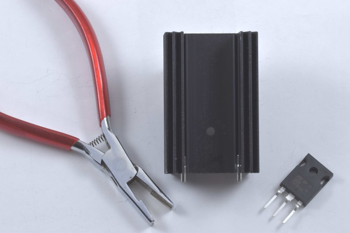
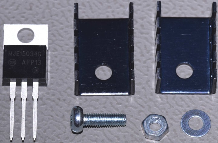
Make thermal reliefs in the leads of the 4 power transistors. One way is using special pliers, see next photo, but pliers with round jaws can also be used. Place the bends as close as possible to the package of the transistors. The heatsinks have a pre drilled hole and there’s not much room for error. Of course you could drill a 3 mm hole a bit above the existing one.
Now place the heatsinks on the PCB. Easiest way is placing the four heatsinks on the PCB and turn everything upside down. Solder the two pins per heatsink while pushing them toward the edge of the PCB (the holes for the pins are a little bit larger) and make sure the heatsink remains perpendicular to the PCB, check this after soldering.
Put a very thin layer of thermal grease (heat transfer compound) on the back of the power transistors. The thermal reliefs in the leads of the 4 larger power transistors should have been made already. Place each transistors against the heat sink, one at the time. Use a 10 mm M3 screw to fix the transistor and place the head of the screw on the outside and the nut on the side of the transistor. Place two M3 washers under the head of the screw. This way the screw is just long enough to go inside the nut but won’t protrude any further. The nearby decoupling 1000 µF capacitor is close the transistor and the screw shouldn’t touch it. Turn the screw real tight and do this for the three other power transistors. Only then solder the leads of the power transistors.
The large 1000 µF decoupling capacitors can be placed on the PCB and soldered. Be sure they are placed perpendicular and don’t touch the nuts/screws of the power transistors.
Transistors T4 and T10 with their small heatsinks can be fitted. Two small heatsinks per transistor are used back-to-back to reduce thermal resistance.
Put some thermal greased on the back of T4 and T10 and on one of the heatsinks per transistor.
Now place the back of the two heatsinks against each other and fasten the transistor real tight with the M3 screw, washer and nut to the two little heatsinks.
Now solder the last two transistors T4 and T10 and vertically placed 5 W resistors R11,R12, R13, R29. R30 and R31.
Test setup:
VTX-146-300-235 transformer (300 VA, 2 x 35 VAC)
2 x 10000 µF per supply voltage (so 20 mF on each side)
SB352 bridge rectifier
At low levels a very small improvement can be seen in the frequency spectrum, in comparison with the SMPS800RE power supply.
Harmonic distortion plus noise:
0.0007 % (1 kHz, 1 W, 8 Ω, B = 22 kHz)
0.0013 % (1 kHz, 1 W, 8 Ω, B = 80 kHz)
The FFT plot shows the frequency spectrum at 1 W in 8 Ω. The switching artifacts of the SMPS are gone. But the rest of the spectrum is essentially the same.
Specifications
(both regulators)
Input voltage range 52 V (low power usage)…43 V
Output voltage range approx. 38,9…41,4 V (theoretically)
38.6…41.1 V measured
Dropout voltage at 6 A 42 V
Dropout voltage at 9.5 A 43 V
Dropout voltage at 13.5 A 44 V
Max. current 15 A peak (half sine wave)
4.8 A average
SOAR protection 15 A at 45 V in
Ripple rejection >60 dB (5 ADC)
No-load input current 27 mA (52 V in)
Bill of materials
Resistor
R1, R19 = 4.7 kΩ, 1 %, 0.6 W
R2, R21 = 150 kΩ, 1 %, 0.6 W
R3, R20 = 12 kΩ, 1 %, 0.6 W
R4, R22 = 3.3 kΩ, 5 %, 1 W, body size 5 x 12 mm max
R5, R23 = 47 Ω, 1 %, 0.6 W
R6, R7, R16, R24, R25, R34 = 1 kΩ, 1 %, 0.6 W
R8, R26 = 300 Ω, 1 %, 0.6 W
R9, R27 = 15 kΩ, 1 %, 0.6 W
R10, R28 = 100 Ω, 1 %, 0.6 W
R11, R12, R13, R29, R30, R31 = 33 Ω, 5 %, 5 W, body diam. 6.4 mm max (axial, mounted upright)
R14, R15, R32, R33 = 0.1 Ω, 10 %, 5 W (body 7.8 x 25 mm max.)
R17, R35 = 6.8 kΩ, 1 %, 0.6 W
R18, R36 = 22 kΩ, 1 %, 0.6 W
P1, P2 = 500 Ω, 0.15 W, trimmer, top adjust
Capacitor
C1, C11 = 22 uF, 20 %, 63 V, pitch 2,5 mm, diam. 6.3 mm max.
C2, C5, C12, C15 = 10 nF, 10 %, 100 V, ceramic X7R , pitch 5 mm
C3, C13 = 15 nF, 5 %, 100 V, PET, pitch 5 mm
C4, C14 = 47 nF, 10 %, 50 V, ceramic X7R, pitch 5 mm,
C6, C7, C16, C17 = 1000 uF, 20 %, 50 V, pitch 5 mm, D 12.5 mm, 5000h@105°C
(EEUFC1H102L, Panasonic)
C8, C9, C10, C18, C19, C20 = 100 nF, 10 %, 100 V, pitch 5 mm, ceramic X7R
Semiconductor/Valves
D1, D2, D4, D5 = SD101A SB00018/D8, DO-35
D3, D6 = HTR20L120CT, TO-220
LED1, LED2 = LED, green, 5 mm (T-1¾)
T1, T2, T9 = BC546B, TO-92
T3, T7, T8 = BC556B, TO-92
T4 = MJE15035, TO-220
T5, T6 = TIP36C, TO-247
T10 = MJE15034, TO-220
T11, T12 = TIP35C, TO-247
IC1, IC2 = TL431BCLPG, TO-92
Other
K1, K2, K3, K4, K5, K6 = Faston PCB tab, two pins, hole diam. 1.4 mm, 6.35 x 0.83 mm
F1, F2 = Fuse clips, 20 A, Littelfuse 01000020Z, for 5x20mm, 2 per fuse
F1, F2 = Fuse, Cartridge, fast acting, 15 A , 5 x 20 mm
HS1, HS2, HS2, HS4 = heatsink MC33271 (for T5/T6/T11/T12), 2.7 °C/W
4 x heat sink FK231SA220, 24 K/W (for T4/T10, two each)
10 x M3 washer, plain, steel
6 x M3 screw, 10 mm, pan head
6 x M3 nut
The Fortissimo-100 high-end audio power amplifier (https://www.elektormagazine.com/labs/fortissimo-100) works best with a regulated +/-40 V power supply. The classical power supply consisting of a transformer rectifier and large smoothing capacitors is not advised as is explained in the text of the Fortissimo-100. For those who don’t like switched mode power supplies here’s a linear regulator with all through hole components, like the amplifier. Maybe the schematic will give a familiar impression. For the voltage regulator to work without drop-outs the input voltage of the circuit must of course be at least 3 V higher, and in case of possible mains voltage fluctuations even more (most SMPS have a wide AC voltage input range). A linear regulator is less efficient compared to a SMPS and a large transformer must be used, and it must have a higher power rating then without the linear regulator. Most transformers have the same standard secondary voltages. To create +/-40 VDC directly a 2 x30 VAC transformer is the most likely choice. The no-load DC voltage is usually around 42 VDC then, largely depending on regulation of the transformer (the no-load output voltage of a transformer is always a few percent higher) and voltage drop across the bridge rectifier. The next higher standard voltage is 35 VAC and results in approximately 49..50 VDC or more with low power, almost 52 V in a test setup).
At a 8 0hm load (at the amplifier output) the regulator would need only a low smoothing capacitance. Advantage of the larger ripple voltage is a somewhat lower power loss in the regulator. But at lower impedances the ripple should not go beyond the drop-out voltage (43 V at 10 A). In practice a 2 x35 VAC ring core transformer of 300 VA with 20000 µF smoothing capacitance was enough as a power supply for the regulator. Maximum (almost clipping) sine wave power at 20 Hz and 0.1 % THD+N in a 3 Ω load caused only a drop-out peak voltage of 1.8 V (dip at the outputs of the power supply). Mind you, continuous output power is 227 W then in the 3 Ω load and the 300 VA transformer is slightly overloaded! This however was not enough to trip the protection of the amplifier and everything keeps working normally.
To make building of this project easy each of the power transistors in the output stage and their drivers have their own heatsink. So there’s no need to drill 6 holes in one common heatsink.
Schematic
Figure 1. Schematic 220581-1 v2.0 Voltage Regulator for Fortissimo-100 Audio Power Amplifier
The basis of any voltage regulator is measuring the output voltage and comparing it to a reference voltage and controlling the output stage accordingly. This circuit follows the same concept. A contrast with standard regulators is the much higher (here the secondary) reference voltage, a little over 33 V, close to output voltage of 40 V. The higher the reference voltage, in this case the measured voltage was 33.6 V, the more the internal gain of the simple circuit, a single differential amplifier, can be used to increase ripple rejection of the input voltage and increase output voltage regulation. Simply put, the circuit consists of a reference voltage, a differential amplifier and an output buffer. Additionally a safe operating area protection is added to both regulators. Let’s look at the positive regulator.
The reference voltage
The reference voltage is not created by a Zener diode. Standard ones have high temperature coefficients. Special temperature compensated versions are hard to come by, especially 33 V versions. Instead an adjustable precision shunt voltage reference is used of type LM431. It has a maximum working voltage of 36 V. Its internal reference voltage (so primary reference voltage of the 40 V regulator) is typically 2.495 V. The cathode current through the LM431 is set by resistor R1. If the input voltage is between 43 and 50 V the current is set between 1.9 mA and 3.4 mA and proved to be sufficient to provide a stable 33.9 V reference voltage. The 33.9 V is set by resistors R2 and R3:
VKA = 2.495 * (1 + R2/R3) + IREF * R2
The adjust current IREF of the LM431 is typically 1.8 µA, so the reference voltage is theoretically 33.95 V then. But this is specified at a cathode current of 10 mA. In the prototype this current is lower and so the voltage is slightly lower, 33.55 V was measured. The LM431 is decoupled by C1. C2 improves stability.
The differential amplifier
The differential amplifier is minimalistic and consists of T1 and T2 and R4 as a current source The voltage at the base of T1 is fairly constant and thus the voltage across R3, neglecting the slightly varying voltage across the base emitter of T1 and D1 with temperature. Schottky diodes D1 and D2 limit a possible reverse voltage of the base-emitter voltages of T1 and T2. To reduce the influence of the voltage drop across each diode and not affect the input offset voltage of the differential pair, due to changes in temperature, they are placed next to each other on the PCB and both will have the same temperature. A few millivolts offset or even tens of millivolts, also caused by differences of T1 and T2, have no real effect on the much higher 40 V output voltage. Even an offset change of 30 mV is less than 1 % variance in the output voltage and is inconsequential for the working of the power amplifier. The voltage across collector resistor R6 is used to drive the output stage. R5 and C3, and also C4 and C5, form the frequency compensation to make the regulator stable, even if the SOAR protection T3/R7/R8/R9 is active. Divider R13, P1 and R14 measure the output voltage and are the negative feedback for the differential amplifier. To compensate all tolerances the output voltage range of P1 is approximately 38.6 V to 41.1 V. With the potentiometer in center position the output voltage is very close to 40 V.
The output stage
Although there are transistors that can handle the maximum output current, needed here when a constant 50 V input voltage is applied, two transistors (T5/T6) are chosen to limit power dissipation per transistor, have a larger overload range, lower drop-out voltage and greater safe operating area to reduce the risk of damage to the output stage in case there’s an overload condition or even a short circuit. The larger PNP power transistors are of type TIP36C (NPN TIP35C in the negative regulator) and are available from several manufacturers. PNP transistors are used in the positive regulator to make the minimum voltage drop of the output stage as low as possible, the base currents flow toward ground. The drop-out voltage is the sum of the saturation voltage of the transistors and voltage drop across the emitter resistors. A lower value for the emitter resistors would reduce the drop-out voltage a little but the currents through the two transistors can become too different then. At high collector currents the gain of the transistors is very low and an additional transistor (T4) is needed to buffer the output of the differential stage. To prevent the saturation voltage of T4 increasing the drop-out voltage of the output stage its collector is connected to ground through a series connection of resistors. This limits power dissipation of T4 and only a very small heatsink is required. However, there’s a catch doing this. Should by what ever cause the input voltage fall below the drop-out voltage T4 will conduct permanently and the dissipation in its collector resistor will be quit high: in case of 100 Ω and 40 V input voltage 16 W. But this will or should never occur!. But just in case, to prevent a burn out of this collector resistor three 5 W resistors are used. To save space they are placed upright. An additional advantage of this collector resistor is a limit to the maximum base current of T5 and T6 and forms a simple current limit. The real protection is formed by T3. The output current is measured by the voltage drop across the emitter resistor of T5 by voltage divider R7/R8 and it drives the base of T3. When for instance the current through R14 is about 7 A, total output current is 14 A. Maximum expected output current is a little over 12 A peak (3 Ω load at the output of the amplifier). T3 will start conducting and due to R9 even sooner depending on the voltage across T5. The exact level where T3 starts conducting is temperature depending and will be sooner the higher the temperature. An additional protection. With music this won’t be an issue. D3 protects the output stage in case the input voltage is suddenly disconnected or short circuited. T5 and T6 are each decoupled with a low ESR 1000 µF capacitor. LED1 indicates the presence of the 40 V output voltage. The input is protected by a 15 A fuse. The maximum RMS current must be taken into account and with a maximum half wave sine current the RMS value is Ipeak/2, so 6,5 A. But, at very low frequencies like 16.4 Hz (if you like organ music) the peak current lasts for several milliseconds, and what is the best fuse rating then? To make sure, even in an overload condition, the fuse won’t blow a 15 A fuse is chosen. The voltage drop across the fuse is also lower. If much more power is taken by the amplifier and/or the regulator the primary fuse of the transformer will/must blow. The 15 A fuse will blow should there be a sudden short circuit behind the fuse .
PCB and heatsinks
This voltage regulator consists of two independent regulators with a common ground. The reference voltage circuit for the negative output voltage is the same as in the positive regulator, but the resistor R19 that sets the current is connected on the other side of the LM431. The common ground connection of the reference IC1 and IC2 and feedback resistors R17 and R35 are connected to the output ground connector K5 as close as possible. The tracks for the feedback of the output voltages on K4 and K6 are routed alongside these ground tracks to R16 and R34 respectively. To keep the thermal resistance of junction-to-ambient of power transistors T5/T6/T11/T12 as low as possible no insulation is used and the transistor makes contact with their individual heatsinks. This means 80 V is present between the heatsinks of T6 an T12. Never touch any part of the regulator when the input voltage is connected. Disconnect the input voltage when working on the regulator. Also the copper planes underneath the heatsinks are connected to the collectors of the power transistors to minimize resistance to the output. The ground connection from input ground connector K2 to output ground connector K5 is routed on top and bottom using 10 mm wide copper tracks. Also tracks of the 20 A fuse clips of F1 and F2 are routed on both sides. The PCB measures 137.2 x 76.8 mm. With the heatsinks mounted the dimensions of the regulator are 156.8 x 86.7 mm. The heatsinks are purposely placed over the edge of the PCB to maximize airflow. If the PCB is mounted on 10 mm standoffs the total height of the regulator about 76 mm. The footprint of the trimmers allows the use of a simple top adjust single turn trimmer or the use of different type of vertical multiturn trimmers. The input and output connector are vertical spade (faston) connectors for low resistance. The transistors T4 and T10 have their own small heatsinks. Each has two small heatsinks (type FK231SA220, 24 K/W) mounted back to back for lower thermal resistance.
Construction
Start with soldering the lowest parts: small diodes, small resistors, 1 W resistors and the horizontal 5 W resistors.
Figure 2. Lower components soldered
Next trimmers, small capacitors, fuse clips + fuses and faston (spade) connectors. The footprint for the trimmers also permits various types of vertical multiturn trimmers to be used.
Figure 3. Trimmers, small capacitors, fuse clips and faston connectors soldered
Next small transistors, IC1 and IC2, small electrolytic capacitors, LEDs and D3 and D6.
Figure 4. Small transistors, IC1, IC2, C1 and C11, LEDs, D3 and D6 soldered
Make thermal reliefs in the leads of the 4 power transistors. One way is using special pliers, see next photo, but pliers with round jaws can also be used. Place the bends as close as possible to the package of the transistors. The heatsinks have a pre drilled hole and there’s not much room for error. Of course you could drill a 3 mm hole a bit above the existing one.
Figure 5. Heat sink, power transistor and special pliers
to make the thermal reliefs in the leads
to make the thermal reliefs in the leads
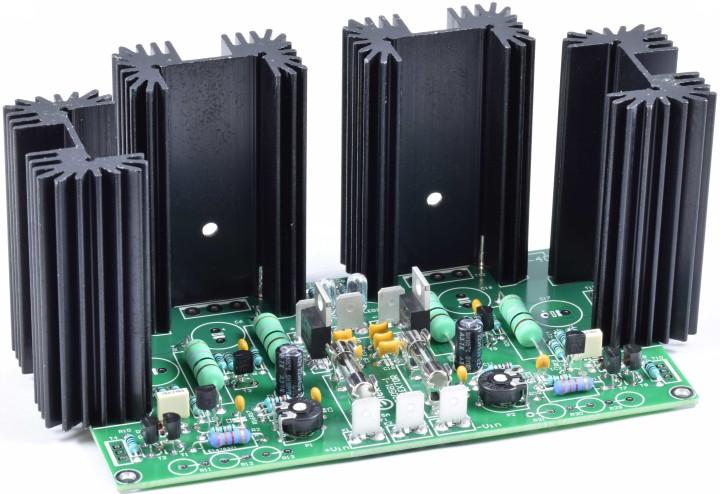
Now place the heatsinks on the PCB. Easiest way is placing the four heatsinks on the PCB and turn everything upside down. Solder the two pins per heatsink while pushing them toward the edge of the PCB (the holes for the pins are a little bit larger) and make sure the heatsink remains perpendicular to the PCB, check this after soldering.
Figure 6. The 4 large heatsinks soldered
Put a very thin layer of thermal grease (heat transfer compound) on the back of the power transistors. The thermal reliefs in the leads of the 4 larger power transistors should have been made already. Place each transistors against the heat sink, one at the time. Use a 10 mm M3 screw to fix the transistor and place the head of the screw on the outside and the nut on the side of the transistor. Place two M3 washers under the head of the screw. This way the screw is just long enough to go inside the nut but won’t protrude any further. The nearby decoupling 1000 µF capacitor is close the transistor and the screw shouldn’t touch it. Turn the screw real tight and do this for the three other power transistors. Only then solder the leads of the power transistors.
Figure 7. Power transistors fitted to the heatsinks and soldered
The large 1000 µF decoupling capacitors can be placed on the PCB and soldered. Be sure they are placed perpendicular and don’t touch the nuts/screws of the power transistors.
Figure 8. The four large 1000 µF decoupling capacitors added
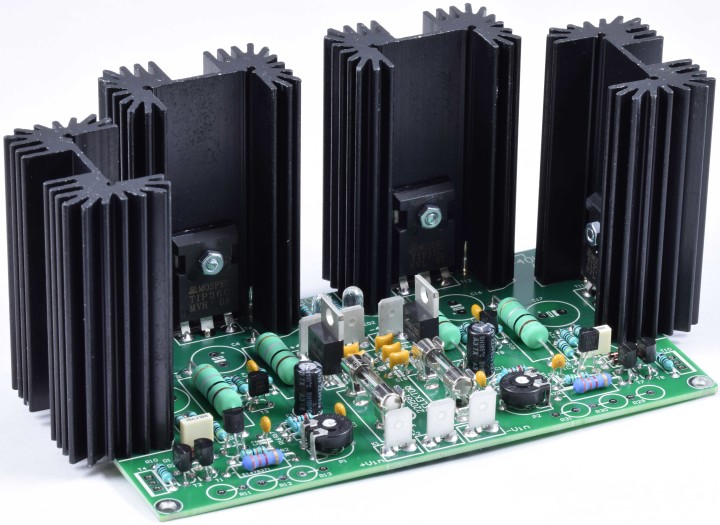
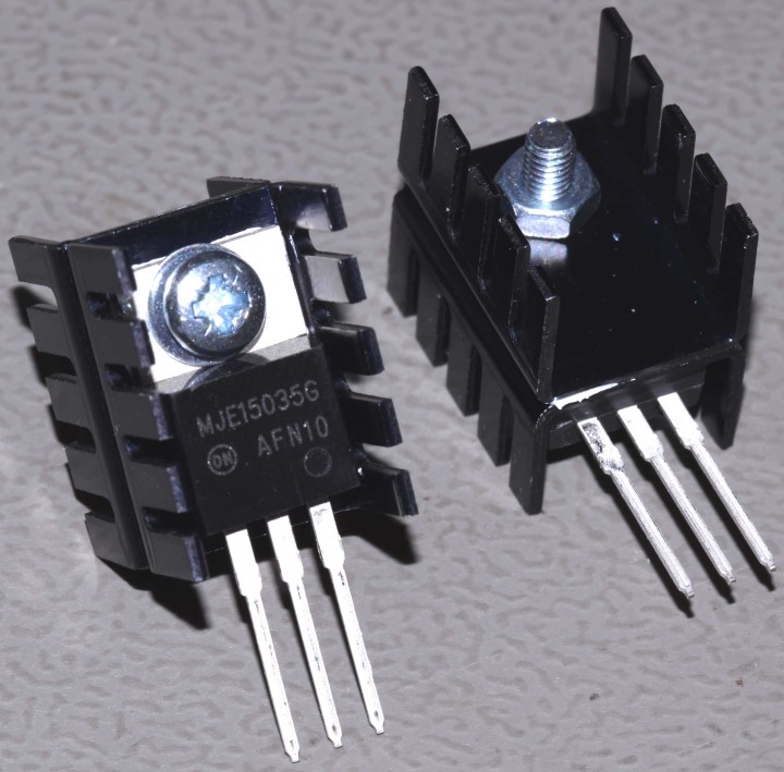
Transistors T4 and T10 with their small heatsinks can be fitted. Two small heatsinks per transistor are used back-to-back to reduce thermal resistance.
Figure 9. The TO220 transistors, two FK231SA220 heatsinks, M3 screw ,washer and nut
Put some thermal greased on the back of T4 and T10 and on one of the heatsinks per transistor.
Figure 10. Thermal grease on the back of the TO220 transistor and one of the heatsinks
Now place the back of the two heatsinks against each other and fasten the transistor real tight with the M3 screw, washer and nut to the two little heatsinks.
Figure 11. TO220 transistors T4 and T10 attached to the little heatsinks
Now solder the last two transistors T4 and T10 and vertically placed 5 W resistors R11,R12, R13, R29. R30 and R31.
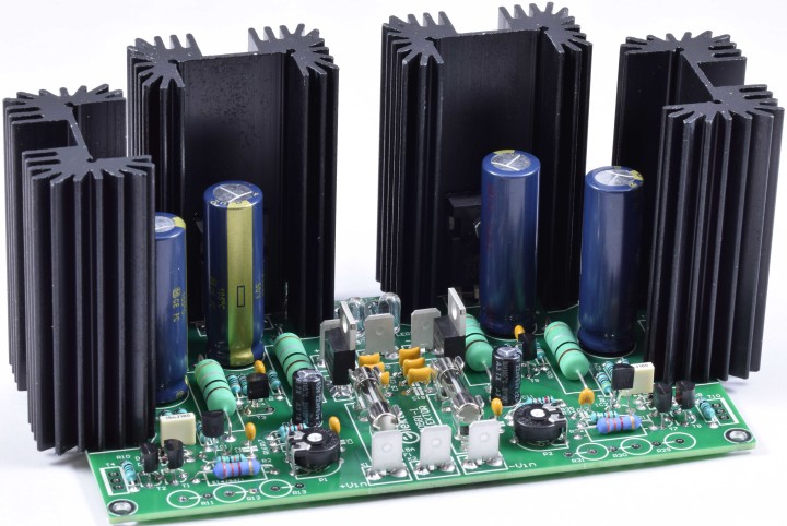
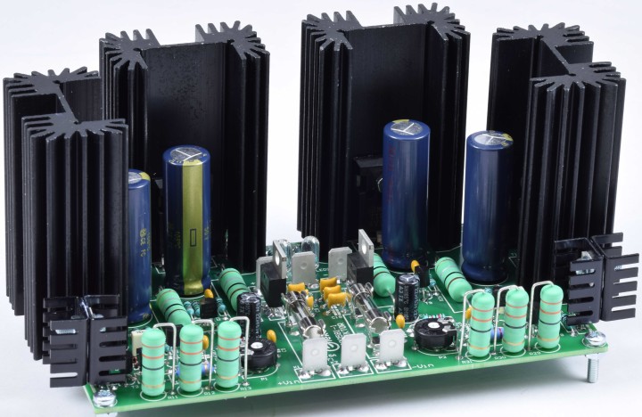
Figure 12. The prototype is ready for testing
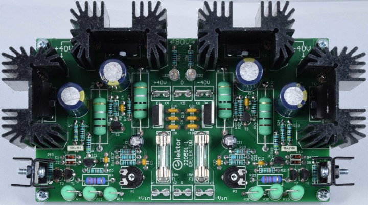
Figure 13. Top view of ready build prototype
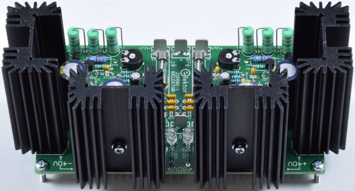
Figure 14. Side view on heatsinks
Test setup:
VTX-146-300-235 transformer (300 VA, 2 x 35 VAC)
2 x 10000 µF per supply voltage (so 20 mF on each side)
SB352 bridge rectifier
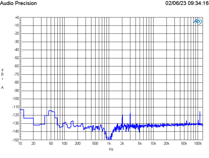
At low levels a very small improvement can be seen in the frequency spectrum, in comparison with the SMPS800RE power supply.
Harmonic distortion plus noise:
0.0007 % (1 kHz, 1 W, 8 Ω, B = 22 kHz)
0.0013 % (1 kHz, 1 W, 8 Ω, B = 80 kHz)
Figure 15. Frequency spectrum Fortissimo-100 output at 1 W in 8 Ω
with linear voltage regulator 220581-1
with linear voltage regulator 220581-1
The FFT plot shows the frequency spectrum at 1 W in 8 Ω. The switching artifacts of the SMPS are gone. But the rest of the spectrum is essentially the same.
Specifications
(both regulators)
Input voltage range 52 V (low power usage)…43 V
Output voltage range approx. 38,9…41,4 V (theoretically)
38.6…41.1 V measured
Dropout voltage at 6 A 42 V
Dropout voltage at 9.5 A 43 V
Dropout voltage at 13.5 A 44 V
Max. current 15 A peak (half sine wave)
4.8 A average
SOAR protection 15 A at 45 V in
Ripple rejection >60 dB (5 ADC)
No-load input current 27 mA (52 V in)
Bill of materials
Resistor
R1, R19 = 4.7 kΩ, 1 %, 0.6 W
R2, R21 = 150 kΩ, 1 %, 0.6 W
R3, R20 = 12 kΩ, 1 %, 0.6 W
R4, R22 = 3.3 kΩ, 5 %, 1 W, body size 5 x 12 mm max
R5, R23 = 47 Ω, 1 %, 0.6 W
R6, R7, R16, R24, R25, R34 = 1 kΩ, 1 %, 0.6 W
R8, R26 = 300 Ω, 1 %, 0.6 W
R9, R27 = 15 kΩ, 1 %, 0.6 W
R10, R28 = 100 Ω, 1 %, 0.6 W
R11, R12, R13, R29, R30, R31 = 33 Ω, 5 %, 5 W, body diam. 6.4 mm max (axial, mounted upright)
R14, R15, R32, R33 = 0.1 Ω, 10 %, 5 W (body 7.8 x 25 mm max.)
R17, R35 = 6.8 kΩ, 1 %, 0.6 W
R18, R36 = 22 kΩ, 1 %, 0.6 W
P1, P2 = 500 Ω, 0.15 W, trimmer, top adjust
Capacitor
C1, C11 = 22 uF, 20 %, 63 V, pitch 2,5 mm, diam. 6.3 mm max.
C2, C5, C12, C15 = 10 nF, 10 %, 100 V, ceramic X7R , pitch 5 mm
C3, C13 = 15 nF, 5 %, 100 V, PET, pitch 5 mm
C4, C14 = 47 nF, 10 %, 50 V, ceramic X7R, pitch 5 mm,
C6, C7, C16, C17 = 1000 uF, 20 %, 50 V, pitch 5 mm, D 12.5 mm, 5000h@105°C
(EEUFC1H102L, Panasonic)
C8, C9, C10, C18, C19, C20 = 100 nF, 10 %, 100 V, pitch 5 mm, ceramic X7R
Semiconductor/Valves
D1, D2, D4, D5 = SD101A SB00018/D8, DO-35
D3, D6 = HTR20L120CT, TO-220
LED1, LED2 = LED, green, 5 mm (T-1¾)
T1, T2, T9 = BC546B, TO-92
T3, T7, T8 = BC556B, TO-92
T4 = MJE15035, TO-220
T5, T6 = TIP36C, TO-247
T10 = MJE15034, TO-220
T11, T12 = TIP35C, TO-247
IC1, IC2 = TL431BCLPG, TO-92
Other
K1, K2, K3, K4, K5, K6 = Faston PCB tab, two pins, hole diam. 1.4 mm, 6.35 x 0.83 mm
F1, F2 = Fuse clips, 20 A, Littelfuse 01000020Z, for 5x20mm, 2 per fuse
F1, F2 = Fuse, Cartridge, fast acting, 15 A , 5 x 20 mm
HS1, HS2, HS2, HS4 = heatsink MC33271 (for T5/T6/T11/T12), 2.7 °C/W
4 x heat sink FK231SA220, 24 K/W (for T4/T10, two each)
10 x M3 washer, plain, steel
6 x M3 screw, 10 mm, pan head
6 x M3 nut
Figure 16. Schematic 220581-1 v2.0 Voltage Regulator for Fortissimo-100 Audio Power Amplifier
Figure 17. Top overlay of PCB 220581-1 v2.0
Figure 18. Copper on top of PCB 220581-1 v2.0
Figure 19. Copper on bottom of PCB 220581-1 v2.0
Want to build a project?
Bring your design to life with the Elektor PCB Service, powered by Eurocircuits. Upload the project files and order professionally manufactured PCBs or assembled boards through a proven European production platform.
Supporting KiCad, Eagle, Gerber, and ODB++ formats, the service is suitable for everything from prototypes and validation builds to series production and volume manufacturing.
Made in Europe. Fast. Reliable. Professional.
Discussion (13 comments)