
IBM Chip uses Graphene FETs
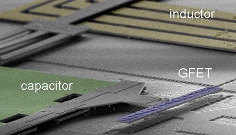
In a paper published in Nature Communications researchers at IBM describe how they have built a silicon-based receiver chip incorporating GFETs or Graphene Field Effect Transistors (the purple structure in the photo) into the circuit. The multi-stage receiver integrated circuit consists of 3 graphene transistors, 4 inductors, 2 capacitors, and 2 resistors.
“This is the first time that someone has shown graphene devices and circuits to perform modern wireless communication functions comparable to silicon technology,” said Supratik Guha, Director of Physical Sciences at IBM Research. In a test the team successfully used the graphene-based receiver to process a digital transmission on 4.3GHz. The binary sequence received was 01001001 01000010 01001101, which represents ASCII coding of the letters IBM.
The data rate with the test chip was just 20 megabits per second but IBM explained that it was not a physical limit of the technology just the test equipment they used. Researchers Shu-Jen Han, Alberto Valdes Garcia, Satoshi Oida, Keith A. Jenkins, and Wilfried Haensch wrote that "One can envision that high-performance graphene radio-frequency circuits will be directly built on top of high-density silicon CMOS logic circuits to form an extremely low-cost, ultra-compact communication system."
Discussion (0 comments)