
Instant Inkjet Circuits
on
Wouldn’t it be ideal if you could just press ‘print’ to produce a printed circuit board? In a paper titled ‘Instant Inkjet Circuits: Lab-Based Inkjet Printing To Support Rapid Prototyping Of Ubicomp Devices’ researchers Yoshihiro Kawahara of the University of Tokyo, Steve Hodges of Microsoft Research and Benjamin Cook, Cheng Zhang and Gregory Abowd of the Georgia Institute of Technology have detailed exactly how it can be done using commercially available products.
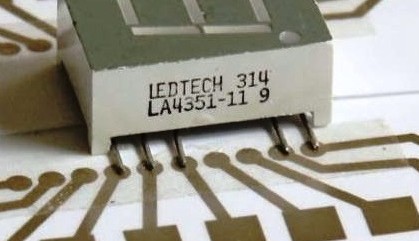
To start off with take a standard inkjet printer, fill its cartridge with silver nanoparticle ink and using a normal PCB layout program, print the PCB layout onto resin coated paper, PET film, photo paper or just plain paper. Once deposited the traces undergo a chemical sintering process as the pattern dries and they become conductive. Components can now be mounted onto the pads using silver-loaded epoxy glue or a type of conductive double-sided tape made by 3M (see picture). The anisotropic property of this tape ensures that it conducts across its thickness and not along its length (like Zebra Strip used for LCD glass connections). The process is also suitable for printing antennae or capacitive, touch detection pads.
For small scale, low-current and low-frequency applications this is an interesting technique to quickly prove a prototype design. Where applications call for a more robust and professional PCB you may need to consider the Elektor PCB prototyper.
Discussion (0 comments)