
Nanowires key to future transistors, electronics
on
A new generation of ultrasmall transistors and more powerful computer chips using tiny structures called semiconducting nanowires are closer to reality after a key discovery by researchers at IBM,
The researchers have learned how to create nanowires with layers of different materials that are sharply defined at the atomic level, which is a critical requirement for making efficient transistors out of the structures.
Electronic devices are often made of ‘heterostructures’, meaning they contain sharply defined layers of different semiconducting materials, such as silicon and germanium. Until now, however, researchers have been unable to produce nanowires with sharply defined silicon and germanium layers. Instead, this transition from one layer to the next has been too gradual for the devices to perform optimally as transistors. The new findings point to a method for creating nanowire transistors.
The findings are detailed in a research paper that appeared last Friday (Nov. 27) in the journal Science. The paper was written by Purdue postdoctoral researcher Cheng-Yen Wen, Stach, IBM materials scientists Frances Ross, Jerry Tersoff and Mark Reuter at the
Whereas conventional transistors are made on flat, horizontal pieces of silicon, the silicon nanowires are ‘grown’ vertically. Because of this vertical structure, they have a smaller footprint, which could make it possible to fit more transistors on an integrated circuit, or chip.
Nanowires might enable engineers to solve a problem threatening to derail the electronics industry. New technologies will be needed for industry to maintain
Transistors made of nanowires represent one potential way to continue the tradition of
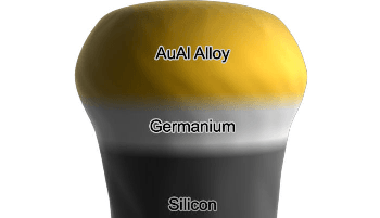
The researchers used an instrument called a transmission electron microscope to observe the nanowire formation. Tiny particles of a gold-aluminum alloy were first heated and melted inside a vacuum chamber, and then silicon gas was introduced into the chamber. As the melted gold-aluminum bead absorbed the silicon, it became "supersaturated" with silicon, causing the silicon to precipitate and form wires. Each growing wire was topped with a liquid bead of gold-aluminum so that the structure resembled a mushroom. Then, the researchers reduced the temperature inside the chamber enough to cause the gold-aluminum cap to solidify, allowing germanium to be deposited onto the silicon precisely and making it possible to create a heterostructure of silicon and germanium.
Having a heterostructure makes it possible to create a germanium ‘gate’ in each transistor, which enables devices to switch on and off.
Source: Purdue News Service
Discussion (0 comments)