
Build Your Own High-Precision Calibrator: -10 V to +10 V, 0 to 40 mA, 0.001%
on

Calibrator Project
I bought a broken oscilloscope on eBay. To take full advantage of its features repairing it, it had to be calibrated with precise voltages and currents. Normally, the calibration values needed are in the range of 1.000 V or 10.000 mA. But for this oscilloscope, according to the calibration procedures provided by the manufacturer, specific voltage and current references were needed: +1.7694 V and -1.7694 V, and 20.253 mA. There are many calibrator solutions on the market, but these devices are way out of my budget or do not have the required resolution and accuracy. So the solution for me was to build my own calibrator.
The Hardware
There are six main blocks in the design:
- Power supply
- Voltage reference
- DAC around the AD5791
- Current generator
- Human Machine Interface (HMI), with its microcontroller
- Heater for stabilizing the voltage reference
The schematic diagram of first five blocks combined is shown in Figure 1. The heater will be discussed later.
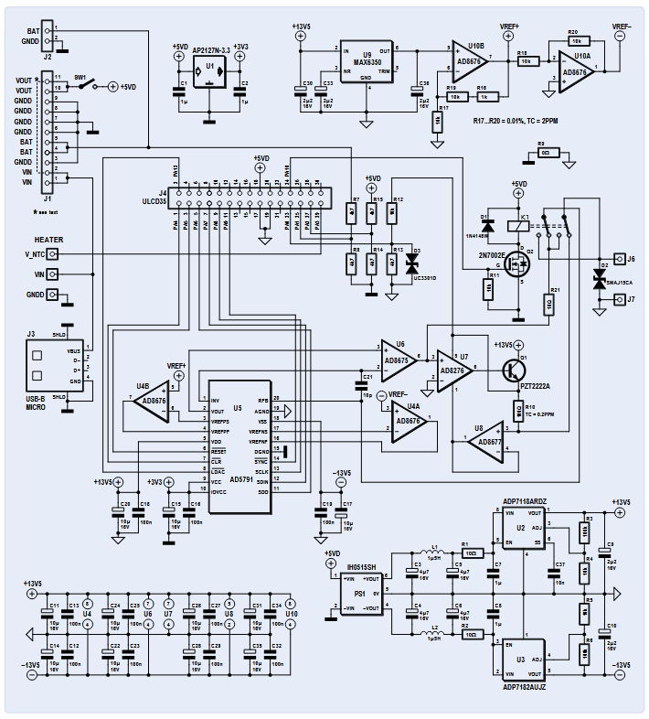
The HMI module provides the user interface and controls the calibrator by setting the output voltage of the DAC. This voltage is also translated into an output current by the current generator; the HMI controls relay K1 via FET Q1, which determines whether the calibrator delivers an highly accurate voltage or current to output terminals J6 and J7. Accuracy is largely determined by the voltage reference, which is a major requirement of this design.
The Power Supply
The calibrator is powered with a USB mains adapter providing at least 500 mA. The 5 V supplied is divided into three separate branches. One powers the HMI with the microcontroller directly. The second feeds U1, a 3.3 V LDO for the logic power supply of the DAC (U5 and around). The third branch is fed to PS1: a galvanically isolated, symmetrical DC/DC converter with +15 V and -15 V outputs. These outputs are filtered and power two linear regulators (U2 and U3). Both regulators are low drop out voltage and low noise types. Their +13.5 V and -13.5 V outputs are used for the output stages of the DAC circuit.
The Voltage Reference
This is the most important and at the same time most critical element in this project. If we need a reference voltage of 10.00000 V with +/- 10 µV accuracy, we would want it to stay at this voltage and precision forever; but in the real world, this is just wishful thinking. The topic of designing accurate and stable voltage references is a science in itself. On the web, there are dozens of articles and specialists who discuss this subject in order to push the limits of features such as: noise, stability in ppm/°C in the short and long term, hysteresis, thermoelectric EMF, piezoelectric etc. In your favorite search engine, look for the Rolls of voltage references: the LTZ1000 with a drift of only 0.05 ppm/°C. Some authors have produced voltage references with amazing and beautiful PCBs with very low temperature coefficient resistors in oil-filled metal housing.
After testing three more affordable voltage references (LTC6655, ADR445, MAX6350ESA), I chose the MAX6350ESA from Maxim, which I found to be the most stable over time with 5 V output. With both op-amps U10A&B inside the AD8676 (dual low noise, low offset drift voltage op-amp) +10.48 V and -10.48 V references are produced (VREF+ and VREF-, respectively). Resistors R16, R17, R18, R19, R20 around the AD8676 are low temperature drift resistors (better than 2 ppm/°C).
The DAC Around the AD5791
The DAC I selected is an AD5791, which was chosen for its 20-bit resolution and 1 ppm linearity. This linearity simplifies the calibration: only the 0 V and 10 V points need to be adjusted. The schematic around the AD5791 uses components identical to the Analog Devices evaluation board for this DAC. In my design the DAC has reference voltages of +10.48 V and -10.48 V, which produces steps of roughly 20 µV. The output voltage can be calculated using:

Or approximately:
The calibrator output voltage is limited in software between -10 V and +10 V. This gives a large capability to compensate the offset error at 0 V.
The Precision Current Source
The four main components of the precision current source are U7 (AD8276 instrument amplifier), Q1 (NPN-transistor PZT1222), U8 (AD8677 precision amplifier) and R10 (100 Ω). Q1 provides the current to the load. This current flows through R10 (shunt resistor), the relay and then goes to the load under test to finally return to ground. The voltage across R10 measured by U8 and U7 is compared to the reference voltage supplied by the DAC AD5791. Output source current equals VDAC / R10, or VDAC / 100. The current is limited to 40 mA by the software to avoid voltage measurement drift in R10 due to thermal heating inside R10 and Q1. The temperature coefficient of resistor R10 is critical and must be as low as 0.2 ppm/°C. For this reason, Q1 is located as far as possible from R10 and of course from reference voltages on the PCB.
The HMI With Its Microcontroller
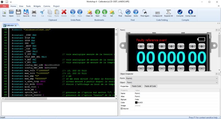
This part is a gen4-uLCD35-DT module from 4D Systems, which combines — among other things — a 3.5” color resistive touch screen, a microcontroller and micro-SD card holder in one module. The 4D Workshop 4 IDE is free and contains the touch button function libraries for this project (see Figure 2). The code itself is a simplified form of C. The Graphical User Interface (GUI) is made as follows: touch buttons and digits are images stored on the micro-SD card. Each image has fixed coordinates on the screen. When the screen is touched, an interrupt is generated and determines which image was touched and triggers the operations that are associated with this “button”.
Heating the Voltage Reference
Output voltage drift versus temperature is measured in ppm/°C. For example, with a 10 V output signal, 1 ppm corresponds to 10 µV voltage drift. The room temperature in my lab roughly varies from 15°C to 25°C, so if the output has a temperature coefficient of 2.5 ppm/°C, the voltage output can change up to 250 µV within this temperature range. I used a DIY thermal chamber with a temperature controller to determine this coefficient.
Then I wondered if I could improve the temperature coefficient if I heated up the voltage reference. I chose a set point at 55°C, way higher than normal ambient temperature. I built a temperature-controlled heater on small PCB and I glued it on the bottom side of the reference circuit of the calibrator. Again, I put the calibrator in my thermal chamber, did a five hour temperature cycle from 15°C to 40°C, and I got a drift of the output voltage of 26 µV, so this gives a temperature coefficient of less than 0.2 ppm/°C, which proved to be five times better than without heater!

A 3D-printed “oven” enclosure was designed to cover the heater and stabilize the temperature of the heater and voltage reference. The 3D design files can also be found on the Elektor Labs page.
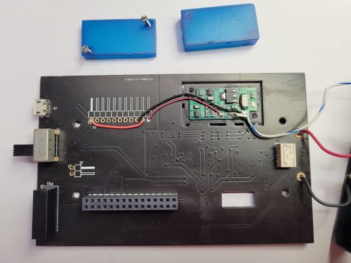
The schematic of the heater control is shown in Figure 3. The NTC (TH1) is placed on the bottom side of the PCB shown in Figure 4 and must be aligned with and glued under the voltage reference U9 on the main PCB.
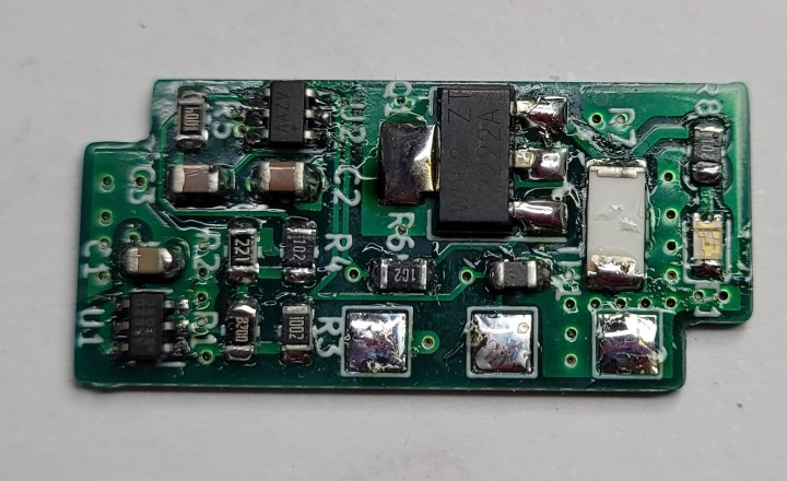
Figure 5 shows the prototype of the heater PCB.
Building the Calibrator
The KiCad design files, the gerber and drill files for ordering the main and the heater PCBs, and the component lists for both boards are available for download on the Elektor Labs web page associated to this project. The software for programming the HMI-module is also available for download on this page.
The project is designed to fit in the Hammond enclosure specified in the Bill Of Materials. Even though soldering SMD parts is not easy for inexperienced makers, it will be not too difficult to assemble the PCBs using a small soldering iron.
Battery Option
The calibrator PCB was designed to be used with a Chinese battery (dis-)charger module (ref DDO4CVSA) from manufacturer Eletechsup and a 4.1 V lithium battery, but after some testing, it was not used in my final design because — in my opinion — it heated up too much. Feel free to try it for yourself, at your own risk of course. Note that Vin and Vout on J1 must be connected with a jumper wire if this module is not installed.
Programming the uLCD35 Module
This calibrator won’t work without software, all the files you need are available for download on the Elektor Labs page [1]. For the HMI module itself, buy the SK-35DT-AR Starter Kit from 4D Systems, which contains the touch display, a 4 GB micro-SD card, and interface to program the HMI module. This kit can be bought from Digikey (1613-1050-ND) or RS-Components (841-7790).Furthermore, you must download and install the 4D system IDE, which is available for free here.

To program the HMI module, first make sure that the micro-SD card is FAT formatted, not FAT32! Download Software.ZIP and USD_FILES.ZIP from [1] and extract their contents to folders on your computer. Copy all files from the USD_FILES folder to the micro-SD card and insert it in the HMI module. Connect the programming interface to the 10-pin header on the module and a USB port on your computer. Open the Program Loader application (see Figure nearby) from 4D system IDE, select the COM port of the programming interface, select Flash as destination, load the file calibrator.4XE and click OK. When the program is loaded, the module displays all buttons and wheels. Note: The source code can be found in file calibrator.4Dg; all comments are in French. The user can edit and modify it with the IDE.
Calibration
As with every reference voltage source, the MAX6350 has to be aged to improve long term stability. I chose 1000 hours at room temperature. After 41 days (about 1000 hours), the reference is stable at 4.99994 V, and the two references of 10.50050 V and -10.49867 V, respectively, are stable at approximately 10 µV.
Then, a minimum 6.5-digit multimeter is required for calibration, and I used my Agilent 34410A for this task. Pressing and holding the Sign button on the HMI for 8 seconds clears all calibration parameters that were previously stored.
Calibrating Output Voltage: First, select the voltage output mode by pressing Volt/mA. Press and hold the 000 button for 5 seconds to start the calibration, a beep sounds and the message calibration mode is displayed. Use the “+” and “-“ buttons of the encoder wheels to obtain 0 V +/- 15 µV read-out on the multimeter, wait about 10 seconds to stabilize. Pressing 000 displays cal stored for 2 seconds, and then the encoder wheels display 10.00000. Then, again using the encoder wheels, select the value necessary to get 10.00000 V +/- 15 µV on the multimeter.
Calibrating Output Current: First select the current output mode by pressing Volt/mA. Press and hold the 000 button for 5 seconds to start the calibration, a beep sounds and the message calibration mode is displayed. The encoder wheels display 00.0100 mA. Using the “+”and ”-“ buttons on the encoder wheels, select the correct value to display 10 µA +/- 100 nA on the multimeter. Pressing 000 displays cal stored on the LCD for 2 seconds, then the encoder wheels display 30.0000. Using the encoder wheels, select the value necessary to generate 30 mA +/- 10 nA.
Operation
The GUI screen consists of a touch-sensitive encoder wheels and three buttons. The +/- buttons of the encoder wheels select the output value. The sign button reverses the polarity of the output voltage, it is inactive in current mode. The Volt/mA button selects the output mode (either voltage or current), and the 000 button resets the output to 0 V or 0 mA, respectively.
The Calibrator: A Valuable Asset
The total costs to build this high-precision voltage and current calibrator will be around €300/$350, which is really a nice price for this device. Admittedly, you’ll also need a high-precision, well-calibrated multimeter to ensure accurate adjustment; this may be an issue, but most of us will somehow, some way have access to this kind of equipment. This calibrator will certainly be a valuable asset to your lab for testing and adjusting all kinds of electronic circuits, devices and measuring instruments.
Editor's Note: This article (210208-01) appeared in Elektor November/December 2021. It is based on the project that Vincent Gautier presents on the Elektor Labs platform, where more detailed information on his calibrator, including all the software, PCBs plus BOMs, and 3D printer files can be found or downloaded. A video presenting this project can be found here.
Questions or Comments?
Do you have questions or comments about his article? Email the editors at editor@elektor.com.

Discussion (2 comments)