
PCB Layout and Safety: Hints for a Safe, Long-Life Design of Your Boards
on
Compared to wiring, the printed circuit board allows us to organize our designs in a professional, rational and compact manner. However, to ensure its safe operation, some basic physical aspects must be considered when high voltage is present and/or some PCB tracks are subjected to heavy current flows. In this article, we look at what to do, but more importantly, what not to do!
Background
The printed circuit board (PCB) has undoubtedly revolutionized the way electronic circuits are made. The earliest examples of civilian use of PCBs date back to 1948, and since then, the technique for making them has made great strides. If you are particularly interested in the whole evolutionary path of the printed circuits’ technology, you can drop by here.
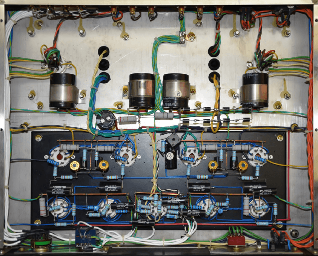
Before the advent of PCBs, the wiring of components was done directly from one to another, taking advantage of their terminal lengths, in air, see Figure 1. The air, as is well known, is an excellent insulator, while the considerable distance between one component and another favored airflow for heat dissipation. All good, then? Not really. The circuits required heavy tin-plated iron frames, the designs often reached massive volumes and weights, and the totally manual construction technique cost a fortune.
But this solution was still viable because electron tube-based devices were still very bulky, and the problem of footprint would not be solved by a PCB anyway.
In the example in Figure 1, which illustrates the bottom view of a KT-88-based vacuum tube amplifier, the layout is quite neat, the power-dissipating components are well ventilated and — being wired in air — the isolation between them is guaranteed, despite the presence of high voltage (800 V DC) in some sections of the circuit.
In addition to the large footprint, the drawbacks of such a wiring solution mainly concern maintenance, especially in the case of components mounted at overlapping levels, which in some cases need to be disassembled only to access the components to be replaced at the lower levels.
With the advent of early, smaller-sized semiconductors, things changed and indeed, the first printed circuit board allowed for smaller, more compact and less expensive designs. This construction approach, however, introduced some problems, chief among them being insulation, heath dissipation, parasitic capacitance and cross-talk among PCB tracks as well as EMI interferences. In this article, we’ll mainly concentrate on the safety aspects, i.e. on high voltage insulation and heath dissipation in general.
Materials
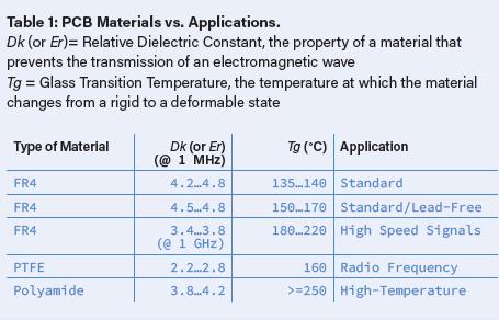
The material used as a base for PCBs can be rigid, flexible, or mixed. The choice obviously depends on the type of application and the expected operating temperature of the circuit. The one most widely used today is a compound of fiberglass and resin called FR4 (Flame Resistant N°4), specified in IPC-4101E Standard. Depending on the purposes, other types of material are also used, as described in Table 1.
Insulation
While PCBs have made it possible to reduce the footprint, the decrease in the distances between conductors has made the insulation aspect more critical, requiring greater care when designing the layout of a circuit. There are many variables to be considered when calculating the minimum distance to be kept between two conductors (tracks, in our case) on the PCB, just to name a few:
- Operating voltage
- Type of dielectric material of the PCB
- Number of layers
- Presence of conductors in the intermediate layers (for PCBs with 3 or more layers)
- Presence of surface coating
- Atmospheric pressure
Therefore, for the sake of time-saving and for dedicating most of our energies to the bulk of the design, it may be useful to use a specific tool such as, for example, the one integrated in KiCad, other PCB CADs or, seeking for something more pro-oriented, heading to Saturn PCB Tool Design Kit, made freely available by Saturn PCB Design Inc. which can be downloaded here.
In Figure 2 we may see the screenshot of the program’s main window, with the multitude of selection tabs available. For evaluating the insulation needs, we may refer to the Minimum Conductor Spacing section, where the calculation algorithm is based on the specifications given by the IPC-2221B Standard.
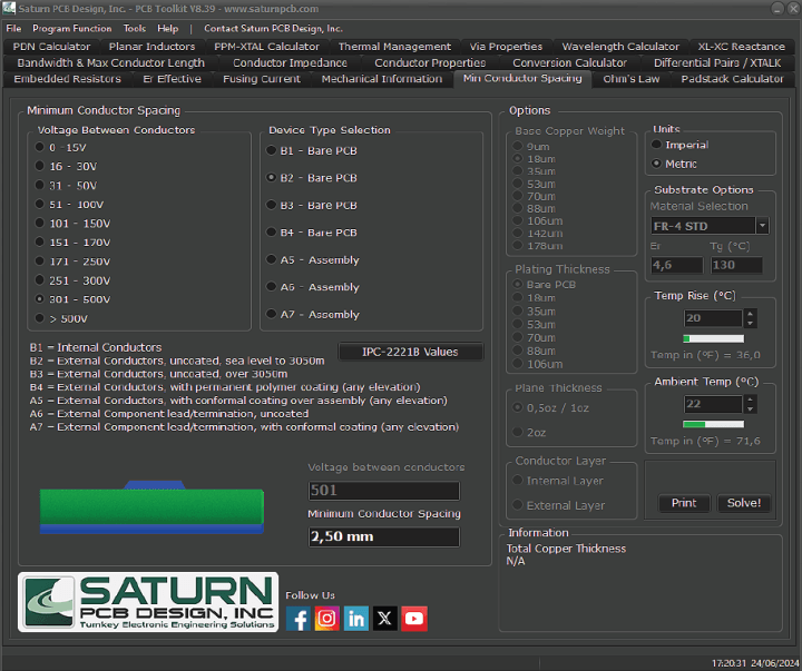
230 VAC and 1.25 mm with 115 VAC input voltages.
One can start by selecting a voltage range from those shown in the table. The values given will apply directly for DC and AC peak voltages; for example, for a mains voltage of 230 V AC, the peak value to be considered will be 325 V and the range to choose 301…500 V.
In the case of voltages above 500 V, it’s possible to select the >500 V option and directly set the value in the Voltage Between Conductors secondary field that is activated further down. After setting the value, the Solve button has to be clicked to get the result.
Then select the B2 option, one of the seven available in the Device Type Selection menu, that relates to an uncoated PCB layout, and standard altitudes above sea level. A short explanation of the different choices is readable just below it.
By selecting the different options (for the same voltage), it is possible to check immediately what is the minimum distance to keep between conductors. For the mains voltage in the above example, the system shows a value of 2.5 mm.
Note: it can be seen that for operating heights above 3050 m the distance increases quite consistently, since high atmospheric pressure is of utmost importance in limiting arcing phenomena. If the circuit we are designing is to be used at high altitudes, it is necessary to protect it with a layer of insulating coating, rather than just relying on the distance between tracks.
Keep The Distance!
Having established what the minimum distance is for our case, let’s see how to put it into practice on the PCB, using connectors that allow to detach the wiring when necessary and excluding cases of direct (soldered) connections to the board.
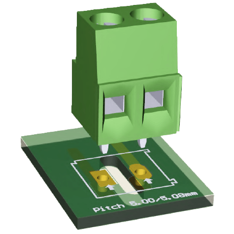
Screw terminals connectors are undoubtedly the most popular and economical for these uses. They exist in different pitches: 2.5/2.54 mm, 3.5/3.81 mm, 5.00/5.08 mm and 7.5/7.62 mm, to name the main ones. To maintain a conductor spacing of 2.5 mm, we can immediately rule out the first two, while for the 5.00/5.08 mm pitch (see Figure 3) some considerations need to be made.

a high-voltage input of 230 VAC. With the arrangement shown in this example,
there’s still the opportunity of using it where the mains voltage is 100 or 115 VAC.
The distance L (marked in red) between the two lower pads is approximately 2 mm, less than the required limit, so this size of connector cannot be used with a mains voltage input of 230 V AC, unless special solutions are applied to PCB routing.
In fact, in case of overall limited space, this connector can still be used, provided the PCB dielectric between the contacts is modified. How? By replacing it with air, as shown in Figure 4. Here the pads’ shapes have been modified and a 2 mm slot milled in between them. This slot will have to extend to the point where the tracks will be — on the PCB route — at least the minimum required size apart.
where these cutouts are also used to separate areas with large potential differences.
Anyway, this is a compromise solution which should be avoided if space exists for larger connectors. Slots and cutouts are often used to further increase the isolation between the high-voltage area on a PCB and the low-voltage one, including ground planes that are usually at earth potential.
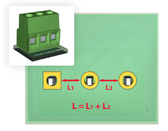
Another practical solution (Figure 5) is to use three contacts of a 5.00/5.08 screw terminal without connecting the center one. In this application, the isolation distance L = L1 + L2 allows the connection to the mains voltage, provided the center pin is not connected to any wire or PCB track and stays floating. Again, this has to be considered as a trade-off design solution.
tracks (floating), the insulation distance doubles, and applying 230 VAC
mains voltage to the input becomes a viable option.
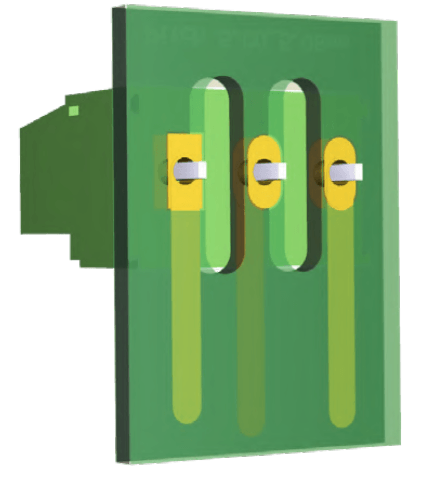
Figure 6 shows another configuration with a 5.00/5.08 mm 3-pole screw terminal, with two slots milled in between the pads. This configuration allows the connection to a standard 230 V AC mains line with L, N and GND, in mind all the safety considerations already made for the previous cases.
with double milling. This solution allows the connection to a
230 VAC mains line with L, N and GND.
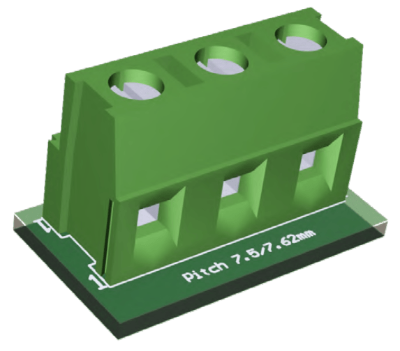
Finally, Figure 7 shows a no-compromise solution, adopting a 7.5/7.62 mm pitch screw terminal block. Its footprint is around 16 mm in a 2-pole configuration and 23 mm in 3-pole. Definitely, it’s not a miniaturized connector, but certainly among the safest ones in terms of isolation and load capability. Its wide pitch allows for any kind of routing and enables the application of voltages even higher than the mains ones.
no special arrangements and also allows the input of higher voltages than the mains one.
Fastons, or spade connectors, are widespread and commonly used. They offer many positive features such as cost-effectiveness, contact reliability, and vibration resistance. In contrast, their installation on PCBs requires careful pad design and excellent solder quality. Furthermore, the m/f insertion force that these connectors require must be compensated for with suitable mechanical supports for the board so that it does not flex during insertion. The minimum recommended board thickness for this application is 1.6 mm.
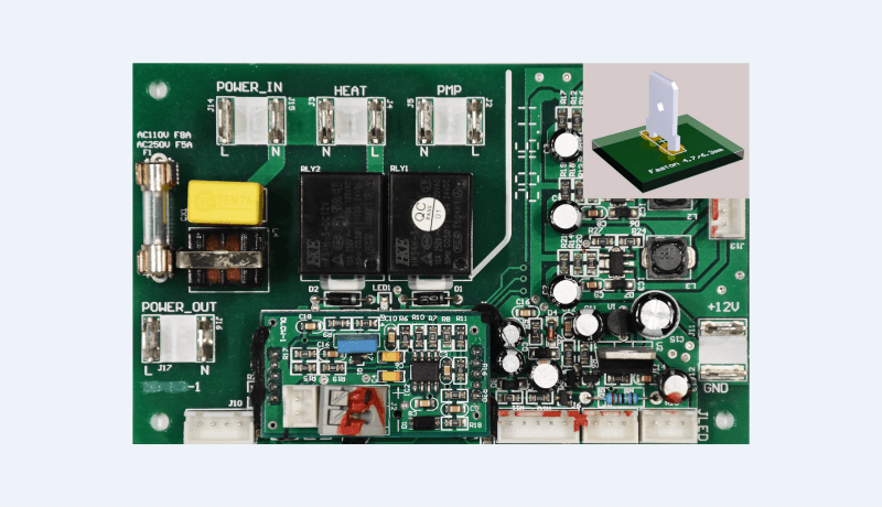
Figure 8a and Figure 8b show, respectively, the component and the solder sides of a sample PCB from the author’s lab.
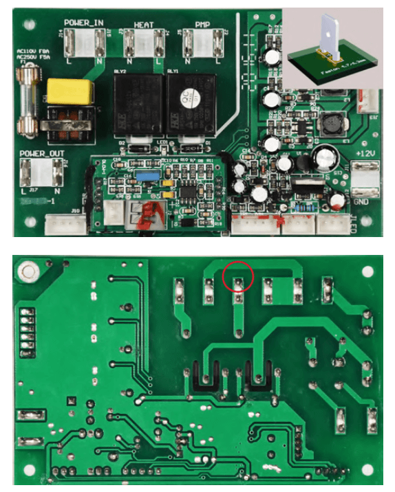
corner is a 3D representation of the power faston type used on it. Note the wide
spacing between the connectors and the white demarcation line between the high voltage
and low-voltage sections. On the solder side, the large reinforcing solder on the faston pads are
evident, as are the U-shaped insulation millings near the relays. Note the minimum
distance (2.5 mm) between N and L at the point circled in red. (Source: author’s lab)
On the left area of the component side note the four pairs of male fastons intended for high voltage connections, on the right a pair used for low voltage input. The silkscreen printing correctly indicates, with a thick white line, the boundary between the high-voltage and low-voltage areas. However, the indication “Danger - High Voltage” is missing.
The solder side of the PCB shows the fastons’ support pads, which were designed without a solder mask. This choice increases the soldered area and consequently the mechanical strength of the joint. The contact spacing is wide, with one (red-circled) exception, where the distance between tracks is 2.5 mm, the bare minimum according to the IPC-2221B Standard. Another good, yet necessary, insulation solution, was applied through the two U-shaped millings between the high-voltage connections of the relays and the respective pads connected to the low-voltage windings.
Keep It Cool!
Another of the safety aspects to consider in the layout of a PCB concerns thermal dissipation. In an electrical or electronic circuit, conductors are subject to heating as a result of the current flow, due to a physical phenomenon known as Joule Effect, about which you can find more information in the next section of this article.
For a proper thermal management of a PCB, the heat produced must be dissipated to keep the circuit within an acceptable temperature range during operation. Ambient temperature and ventilation are key factors and are the basis for any further thermal evaluation in the design phase.
Let’s take a look at the Conductor Properties tab in Saturn PCB Toolkit (Figure 9), where the most relevant parameters have to be input and the options for our purposes chosen. For PCB type selection:
- Material Selection
- PCB Thickness
- Base Copper Weight
- Plating Thickness
- Bottom Copper Layer (yes/no)
For the track sizing:
- Conductor Width
- Conductor Lenght
- Parallel-Connected Conductors
Environmental parameters:
- Ambient Temperature (°C)
- Temperature Rise (°C)
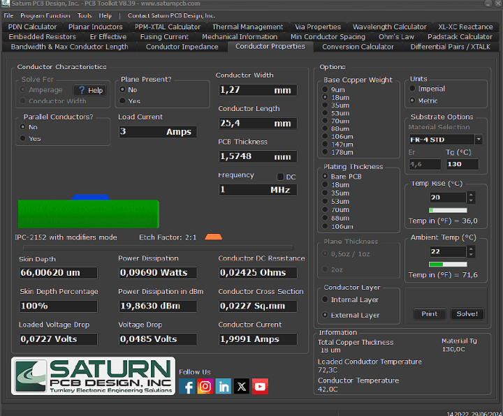
a current of 3 A that (according to IPC-2152 Standard) is rated for a maximum of 1.99 A.
Some re-engineering is needed here!
Suppose we have a 1.6 mm-thick FR4-STD-type PCB, with an 18 µ, single-sided, un-plated (bare) copper layer, and we want to evaluate the thermal performance of a 1.27 mm wide, 25.4 mm long track that is to carry a current of 3 A. From reading the results, which are obtained by pressing the Solve button after entering the necessary parameters, we see that according to the IPC-2152 Standard our track guarantees a rated current of 1.991 A (Conductor Current, on the menu), while our requirements call for 3 A. The rated current value is calculated for a standard temperature rise of 20°C, that with an initial ambient temperature of 22°C will lead to a final operating track’s temperature of 22 + 20 = 42°C.
With a kind of reverse engineering, the program allows us to simulate a possible end situation. Assuming we wanted to maintain the current of 3 A on our track — without varying its electrical properties (resistance) — clicking on Temp Rise to increase the value until the readout in the Conductor Current field indicates the value closest to 3 A, we would notice that the thermal rise comes up to 49°C, which added to the initial ambient temperature of 22°C would lead to a work temperature of 71°C, too high for a continuous operating condition.
This is even before we have considered the thermal dissipation of all the power components laid on the circuit board — resistors, diodes, power semiconductors, regulating ICs, etc. — whose individual contributions must be added to that of our example. The overall thermal calculation for a PCB requires a complex modeling that is not the subject of this article, but could well be for a next one.
There are several possible solutions to this case, let’s look at some of them.
Increase of the physical size of the track: by increasing the width and/or thickness of the track (by choosing a PCB with a thicker copper layer, or plated, or both), the rated current increases considerably. However, in case of space constraints, increasing the track width must always maintain the insulation conditions between them (minimum distance, as described above), and this solution is not always feasible.
Increase of the track thickness by tin soldering: certainly one of the most practical and least expensive solutions. It allows increasing the current carrying capacity of the track, without increasing its width. In Figure 10 there’s a good example, referring to a 12 V switch-mode power supply, where the tracks with a high current flow in both the low and high-voltage areas have been enforced with tin.
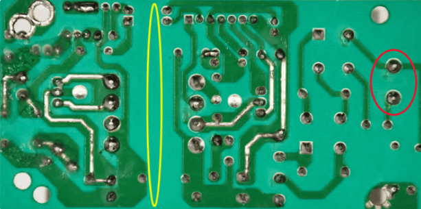
Note the 230 V mains input by a 7.62 mm pitch connector on the right (red) and the wide insulating
area (> 7 mm, yellow) between the low and high-voltage stages of the circuit. (Source: author’s lab)
External copper layer: on PCBs with two or more layers, the bottom copper layer works as a heat sink. Its presence, in addition to being an effective shield for the circuit, helps to dissipate the heat, increasing the thermal performance of the circuit.
Multiple tracks: the current flow can be spread across two or more tracks connected in parallel, with a significant increase in thermal dissipation and thus current flow rate. Saturn PCB Design allows you to set the number of these tracks and performs calculations accordingly.
If there’s enough space on the PCB layout, the track width can be increased in the Conductor Width field, until reading a value close to 3 A in the Conductor Current field; in this case it’s 2.6 mm, which according to the specifications allows a current rating of 3.03 A.
In the case of space restraints, however, the simple solution mentioned above is not viable, the expected current rate of 3 A on the track can be reached by choosing an 18 µ-plated version of the PCB (18 µ copper with a 18 µ coating on it), or heading to a 35 µ thick copper layer instead of the 18 µ one. These choices might have an impact on the budget.
If, on the other hand, the chosen option is thickening the track with tin, it must be kept in mind that after soldering it will not be possible to know the resistivity value of the track by theory, but only in practice, by measuring with a milliohmeter the individual track’s resistance before populating the PCB. This solution may be viable if the number of tracks intended for high currents is very limited, not in other cases, where increasing the thickness of copper and plating is certainly the most professional choice.
This improves the ventilation of the component and reduces the thermal stress on the PCB.
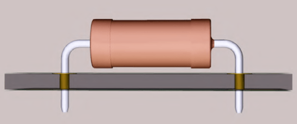
In addition to the heat generated by the power circuit tracks, of course, one must carefully consider components that dissipate non-negligible amounts of energy, such as resistors and power diodes. It is never a good choice to rely on the circuit board to dissipate (partially) by contact the heat generated by a component, unless its shape has been specifically designed for that purpose. In the example in Figure 11, the component is soldered in a raised position relative to the PCB surface. This facilitates convection (air) cooling and prevents stress on the PCB material through contact of small surfaces.
In contrast, in the example on Figure 12, the TO-220 component (left) is mounted on the PCB where a small dissipation area has been provided on the bottom layer (right). This solution is quite practical in cases where the power dissipated by the component is too high for vertical-mount operation without a heatsink, but too low to justify the use of a dedicated metal heatsink, which would increase the footprint.

back layer, to help dissipate the generated heat.
The Joule Effect
In any electrical circuit, when an electric current flows through a conductor, some of the energy is not transferred, but dissipated in other forms of energy, predominantly heat. This phenomenon affects any type of current, direct or alternating, and is known as Joule Effect. To understand why this occurs, we must think of the conductor at a microscopic level. An electric current is given by a flow of charges moving neatly in the same direction, due to the electric field created by a voltage source. The free electrons, moved by the electric field within the conductor, do not follow a totally linear path, but one that is bumpy due to the presence of atoms or molecules in the material’s crystalline lattice, changing direction and releasing some of their energy to the constituents they impact. The latter absorb the energy released by the electrons and increase the oscillation motion around their equilibrium positions; as a result, increased agitation of atoms and molecules corresponds to a rise in the temperature of the conducting material. In certain applications, such as in air or water electrical heating devices, or incandescent filament light bulbs, for example, this phenomenon is sought intentionally, to convert the maximum amount of electrical energy into heat. In electronic circuits — on the other hand — the Joule effect has to be minimized, to ensure the safe operation of a design.
Before Wrapping-Up
Before closing our technical roundup, I think it is useful to mention that the IPC-2221B Standard to which few of the examples in this article have referred is the least restrictive in the industry about insulation, and the prescribed distances cannot be reduced. For critical applications, such as certain types of household appliances or for medical designs, there are other more stringent standards such as, for example, IEC 60335, which we encourage you to consult depending on your project needs.
I would like to thank Marco Castiglioni, a talented professional in routing printed circuit boards for industry, for preparing all the 3D material and especially for his tireless work as a consultant in the writing of this article.
Editor's note: This article (230570-01), which appeared in Elektor Nov/Dec 2024, is by Roberto Armani (Elektor) and Marco Castiglioni (Italy). Mr. Castiglioni is an engineer with a degree in electronics. After his studies, he started working as a PCB layout design engineer at an important Italian Professional Audio Company, where he began to use programs such as Cadstar, Orcad, Protel, Pcad and Veribest. In 1995, he opened his own studio and started working on PCB routing for companies of all sectors (Audio, Medical, Industrial, LED Lighting, Home Automation etc.). After 30 years, he is still active in the market, always keeping up learning and staying up to date with current Regulations and new technologies aimed at the PCB manufacturing sector. You can find him at several comic and movie conventions, dressed as a Klingon, at the Star Trek booth. Visit www.masterista.it for more information.


Discussion (0 comments)