
Power Semiconductor Tester: Tests Power Transistors, SCRs, TRIACs and Diodes
on
The circuit diagram of the power semiconductor tester is shown in Figure 1. S1 is an on/off switch, and S2 changes the supply polarity to the test circuit (for NPN/PNP transistors, N- and P-channel MOSFETs, SCRs and TRIACs). For my tester prototype, I managed to find a center-off switch for S2, so I did not need S1.
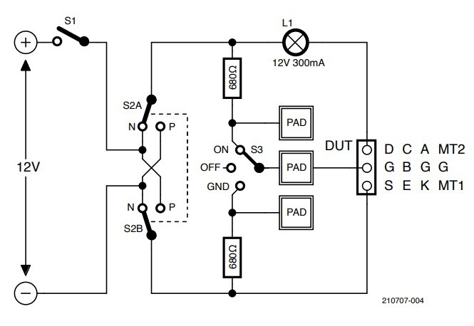
S3 — also a center-off type — applies a voltage and current to the base/gate of the device under test via a 680-Ω resistor. For testing MOSFETs with their high impedance gates, touchpads are also provided, so you can use your finger resistance (usually around 1 MΩ) instead.
When the device switches on, this is shown by a small lamp L1 which limits the current to around 300 mA — enough to show the device is working properly.
Operation
To test a BJT, select the polarity with S2 and connect the device. L1 should illuminate for the ON position of S3, and it should be off if S3 is in the OFF or GND positions.
To test a MOSFET, again select the polarity with S2, and put S3 in the center OFF position. When you touch the two upper touchpads, it should switch on and light L1. L1 will stay lit if you remove your finger. This is due to the gate capacitance of the MOSFET and indicates that the gate insulation is good. Touch the two lower touchpads, and it should switch off. Incidentally, Darlington BJTs may also light slightly with the upper touchpads, especially if you wet your fingers!
To test an SCR, put S2 in the N position. When S3 is ON, the SCR should trigger on and light L1, and will remain on even if S3 is put to OFF or GND. Only when you switch off the supply with S1 or S2 will it go off.
TRIACs are like SCRs, but test them in both polarity positions of S2. Again, they will stay on until the supply is interrupted.
Diodes can be connected to the A and K terminals and will conduct — lighting L1 — for only one position of S2.
Setup
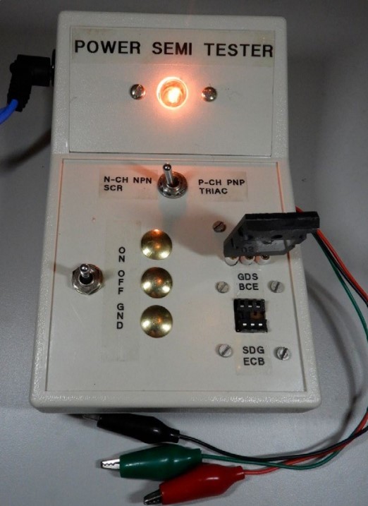
As the circuitry is so simple, point-to-point wiring can be used, using the terminals of the switches and sockets for mounting. For sockets, you can use cut off IC sockets or improvise from other connectors. I put in some test leads to cope with devices that won’t fit the sockets. My finished tester is shown in Figure 2. It’s really handy for testing devices that I’ve removed from old PCBs.
Questions or Comments?
Do you have technical questions or comments about his article? Email the author at stn564@yahoo.com.au or contact Elektor at editor@elektor.com.
Discussion (8 comments)