
140177 NFC Interface
This circuit connects a NXP NFC tag IC (NTAG I2C) with our ECC bus through an ATmega328P controller. As NXP describes it:By combining an NFC interface with a contact I²C interface, the NXP NTAG I²C solutionenables new kinds of NFC tags interactions, including advanced device pairing,personaliz
This circuit connects a NXP NFC tag IC (NTAG I2C) with our ECC bus through an ATmega328P controller. As NXP describes it:
By combining an NFC interface with a contact I²C interface, the NXP NTAG I²C solution
enables new kinds of NFC tags interactions, including advanced device pairing,
personalization of electronic devices, and device maintenance.
There are two versions the NT3H1101W0FHK (1 kB memory) and the NT3H1201W0FHK (2 kB memory).
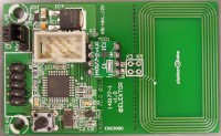
The circuit is experimental and software is being developed. We divided the circuit into two parts. A main PCB with the antenna, micro-controller and ECC connector. And a very small PCB with the size of an 8 pin DIP IC as a break-out-board. Only the NTAG I2C IC and a capacitor are on it. This very small IC is described as a NFC Forum type 2 Tag compliant IC with I2C interface. It’s only 1.6 by 1.6 mm and 0.5 mm high. Soldering it is not for the faint-hearted. It is a QFN style IC with eight 0.2 mm (typical) pads underneath at 0.5 distance (XQFN8: plastic, extremely thin quad flat package; no leads)! On the BOB is also a capacitor (C1) for tuning the antenna to exactly 13.56 MHz. In our prototype the capacitor needed is 18 pF (value for maximum sensitivity). We used the one on the BOB, easier access there. For fine tuning a second capacitor is on the main PCB (140177-1), but our experience is that it’s not that critical. The BOB is mounted with two headers (round pins) in two sockets on the main PCB. Soldering the BOB directly to the main PCB will most probably change the value of tuning capacitor. The BOB can also be used for other experiments, for instance on a breadboard. We used a function generator and the led D2 connected to the Vout (energy harvesting output) to determine the optimal value. The output of the generator is connected to a flat coil. Changing frequency and increasing the distance from the antenna to the coil will tell if the value is correct. Best resolution is achieved if the led is just turned on. Increase distance and change frequency to find the maximum distance. Changing frequency will turn the led off-on-off and you can estimate the center frequency. Adjust the capacitor if needed.
Jumper JP1 on the main PCB selects the voltage source (5 V). It can be taken form the EEC bus (K1) or an external AC adapter (connected to 5 V regulator IC3). The controller runs on 5 V but the NTAG works on a 3.3 V power supply and has its own little 3.3 V regulator (IC2, SOT23-3). Led D1 and S1 are added for testing or additional features. R7 is for protection in case PD2 from the processor is set as an output.
The antenna is kept at some distance from the rest of the circuit. The antenna can be sawed off along a row of holes in the PCB. But be aware that any change in the connection of the antenna be it through connectors and/or wires will change the tuning capacitor needed!
Bill of materials 140177-1 v1.1
R1,R3,R4 = 10 kΩ, 1 %, 0W1, SMD 0603
R2,R6,R7 = 1 kΩ, 5 %, 0W1, SMD 0603
R5 = 1k5, 5 %, 0W1, SMD 0603
Capacitor
C1,C2 = 22 pF, 10 %, 50 V, SMD 0603, C0G/NP0
C3,C4,C5,C7 = 100 nF, 10 %, 16 V, SMD 0603, X7R
C6 = not mounted
C8,C9 = 1 µF, 20 %, 6V3, SMD 0603
C10 = 4µ7, 10 %, 6V3, Tantalum, SMD 0805 (Case R), ESR 7 Ω
C11 = 10 µF, +80/-20 %, 25 V, SMD 1206, Y5V
Semiconductor
D1,D2,D3 = LED Green, SMD 0805
D4 = PMEG2010AEH
IC1 = ATmega328P-AU, SMD TQFP 32A
IC2 = XC6206P332MR, SMD SOT23-3
IC3 = NCP5501DT50G
Other
K1 = Pin header, 2x5, vertical, pitch 2.54 mm
K2 = Header straight, 2x3, pitch 2.54 mm
K3,K4 = not mounted
K5,K6 = 2-way pinheader SIL, pitch 2.54 mm
JP1 = 3-way pinheader SIL, pitch 2.54 mm
JP1 = Single shunt jumper 2.54 mm spacing
S1 = Switch tactile 6x6 mm SPST-NO, 12 V 50 mA
X1 = Crystal, 16 MHz, 50 ppm, Cload 18 pF, 5x3.2 mm
Misc.
PCB 140177-1 v1.1
MOD1 = 140177-92(?)
Bill of materials 140177-2 v1.0
Capacitor
C1 = 18 pF, 5 %, 50 V, SMD 0603, C0G/NP0 *
Semiconductor
IC2 = NT3H1201W0FHK, SMD XQFN8
Other
K1,K2 = header through hole (4-way) pitch 2.54 mm, round pins (D01-9923246., Harwin)
Misc.
PCB 140177-2 v1.0
* See text
Discussion (3 comments)