
Energy Funnels Boost Solar Cell Performance
on
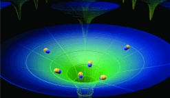
MIT engineers have proposed a new way to improve solar cell performance by using special ‘funnels’ to capture photons. The funnels would be formed in a thin film of semiconductor material by pressure from microscopic needles, producing elastic strain in the funnel area. The strain causes the band gap of the material to vary over the surface of the funnel, which allows a broader spectrum of light to be converted into electricity. The electron/hole pairs produced by the photons in the incident light would also be guided toward the centre of each funnel by electrical forces, improving efficiency compared to the usual diffusion process.
The MIT team used computer modelling to determine the effects of elastic strain on a funnel depression in a thin sheet of molybdenum disulphide (MoS2), a natural semiconductor material that can form films just one molecule thick. The elastic strain, and the corresponding change in the potential energy of the electrons, varies with the distance from the centre of the funnel. The potential energy determines the wavelength of the photons that can be captured by the material, and thus the portion of the light spectrum that can be converted into electricity. The team hopes to carry out laboratory experiments in the future to confirm their theoretical findings.
Incidentally, one of the first practical uses of elastic strain engineering is a technique developed by IBM and Intel that boosts electron velocity in semiconductors by 50 %, simply by imposing a 1 % elastic strain on nanoscale silicon channels in transistors.
Discussion (0 comments)