
Lattice Announces New Low Power FPGA Platform
December 11, 2019
on
on
Lattice Semiconductor Corporation (NASDAQ: LSCC), the low power programmable leader, today announced its new low power FPGA platform, Lattice Nexus™. The platform is architected to deliver power-efficient performance that will benefit developers of a wide range of applications, including AI for IoT, video, hardware security, embedded vision, 5G infrastructure and industrial/automotive automation. Lattice Nexus is built with innovations at every level of design, from solutions, to architecture, to circuit, and delivers higher system performance at significantly reduced power consumption.
“The Lattice Nexus platform augments the parallel processing and re-programmability of FPGAs with the power-efficient performance demanded by today’s technology trends, like AI inferencing at the Edge and sensor management. The platform also accelerates the rate at which Lattice will release future products,” said Steve Douglass, Corporate Vice President, R&D, Lattice Semiconductor. “Additionally, the Lattice Nexus platform offers easy-to-use solution stacks targeting high-growth applications that help customers more quickly develop their systems, even if they are not expert in FPGA design.”
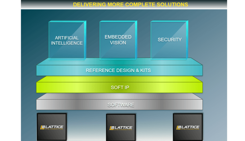
To increase ease-of-use for customers, the Lattice Nexus platform provides innovative system-level solutions that combine design software and pre-engineered soft IP blocks with evaluation boards, kits and reference designs to enable them to build their systems more quickly. These solutions target key growth application areas like embedded vision and include solutions like sensor bridging, sensor aggregation and image processing.
The Lattice Nexus platform has innovative architectural features that optimize system performance at industry-leading low power. For example, the platform’s optimized DSP blocks and higher on-chip memory capacity enable power-efficient computing, such as AI inferencing algorithms, and runs twice as fast at half the power of Lattice’s previous FPGAs.
Lattice Nexus also uses innovative circuit design to deliver key capabilities to customers, including programmable power-performance optimization and very fast configuration for instant-on type applications.
Lattice Nexus is developed on high-volume 28 nm fully-depleted silicon-on-insulator (FD-SOI) process technology from Samsung. This innovative technology features 50 percent lower transistor leakage compared to bulk CMOS, and is the best technology for delivering the low power Lattice Nexus platform.
“We are excited to collaborate with Lattice to bring the benefits of our Samsung Foundry 28FDS manufacturing process technology to the low power FPGA market,” said Ryan Lee, Vice President of Marketing at Samsung Foundry. “By combining their innovation and expertise in FPGA fabric design with our industry-leading and differentiated foundry technology, Lattice will continue its leadership in low power FPGAs for years to come.”
For more information, please visit www.latticesemi.com/LatticeNexus.
“The Lattice Nexus platform augments the parallel processing and re-programmability of FPGAs with the power-efficient performance demanded by today’s technology trends, like AI inferencing at the Edge and sensor management. The platform also accelerates the rate at which Lattice will release future products,” said Steve Douglass, Corporate Vice President, R&D, Lattice Semiconductor. “Additionally, the Lattice Nexus platform offers easy-to-use solution stacks targeting high-growth applications that help customers more quickly develop their systems, even if they are not expert in FPGA design.”
To increase ease-of-use for customers, the Lattice Nexus platform provides innovative system-level solutions that combine design software and pre-engineered soft IP blocks with evaluation boards, kits and reference designs to enable them to build their systems more quickly. These solutions target key growth application areas like embedded vision and include solutions like sensor bridging, sensor aggregation and image processing.
The Lattice Nexus platform has innovative architectural features that optimize system performance at industry-leading low power. For example, the platform’s optimized DSP blocks and higher on-chip memory capacity enable power-efficient computing, such as AI inferencing algorithms, and runs twice as fast at half the power of Lattice’s previous FPGAs.
Lattice Nexus also uses innovative circuit design to deliver key capabilities to customers, including programmable power-performance optimization and very fast configuration for instant-on type applications.
Lattice Nexus is developed on high-volume 28 nm fully-depleted silicon-on-insulator (FD-SOI) process technology from Samsung. This innovative technology features 50 percent lower transistor leakage compared to bulk CMOS, and is the best technology for delivering the low power Lattice Nexus platform.
“We are excited to collaborate with Lattice to bring the benefits of our Samsung Foundry 28FDS manufacturing process technology to the low power FPGA market,” said Ryan Lee, Vice President of Marketing at Samsung Foundry. “By combining their innovation and expertise in FPGA fabric design with our industry-leading and differentiated foundry technology, Lattice will continue its leadership in low power FPGAs for years to come.”
For more information, please visit www.latticesemi.com/LatticeNexus.
Read full article
Hide full article
Discussion (0 comments)