
Modular General Purpose RF Link Using Manchester Code [120049-I]
Frequently there is a need to send data to a distant point without using a wired connection, either because the location’s infrastructure would not allow a twisted pair to link both extremes, or just because one or both of the connected circuits are intended to be portable, or simply wireless.
Frequently there is a need to send data to a distant point without using a wired connection, either because the location’s infrastructure would not allow a twisted pair to link both extremes, or just because one or both of the connected circuits are intended to be portable, or simply wireless.
There are several ways to send data wirelessly, each of them with its own pros and cons; here I will describe a method to send data via Radio Frequency (RF), in the band of 315~433MHz, at a maximum bit rate of 5000bps, using low cost but highly reliable components, and implementing an RF-friendly protocol, the Manchester Code, reaching distances in excess of 600ft.
All difficulties involving RF circuitry have been already solved and the final result will be two general purpose units, one for transmission (TX) and the other for reception (RX), ready to be used in any application, just by changing the code of the included microcontroller.
Creating an RF link involves hardware and software (sometimes called firmware), both at the transmitter end (TX) and the receiver one (RX). Let’s begin by describing the hardware, and later we will go deeper into the software.
Speaking of antennas, this is the other very important - but usually forgotten - element of a successful RF link. A theory about antennas may take a complete book; fortunately this will not be required since Linx Technologies comes with a solution through its antenna division, Antenna Factor. Here again, there are plenty of choices, and I will use the ¼ wavelength monopole reduced height antenna. I like this choice because I have obtained excellent results with these very short antennas, and all of them are of the same height despite the band, so a change of band will not modify the appearance of the final setup.
The bellow schematic represent RF link transmitter and Receiver.
Designing the transmitter (TX):
If you ever had the chance to go over the TX module datasheet, you may have learned that it simply transmits whatever is fed into the DATA pin, within certain restrictions, but there is no intelligence included, i.e. no data synchronism, no code protection, etc.
So, we need to provide such intelligence, adding a microcontroller to our TX unit. Let’s begin with the full circuit schematic. (Check with schematics attachements)
The circuitis fairly simple; only one line connects the microcontroller with the TX module, from PIN A0 (RA0/AN0, pin 17) to the DATA input. You may notice a resistor divider in the middle, formed by R5 and R6; since the microcontroller is fed with 5v and the TX module with 3v, this divider makes the proper voltage conversion. The rest of the components are required for the proper operation of the main ones, but play no active role in the actual data transmission. C3, C4, C5 and C6 are the classic ceramic 0.1µF decoupling capacitors. C7 is a special SMD Tantalum capacitor, rated 10µF/6.3v, intended to be mounted as close as possible to the microcontroller power leads, to reduce any noise produced by this digital component. R4 is intended to keep the microcontroller running (this is the Reset pin, if tied low), and the oscillator is a standard crystal running at 20MHz.
As briefly mentioned before, the TX module works with 3v, but our circuit is fed by a 5v supply (this is an external supply). So, in order to get this regulated 3v, a fixed regulator is used (LP2950-30LPR, by Texas Instruments) adding C2, R2 and C1 for additional stability, as recommended in the datasheets. C1 is made of tantalum, rated 10µF/16v.
Two additional resistors are connected to the TX module. R1 connects the PDN pin to 3v, keeping it high. If low, this pin will place the TX in a low-current state, unable to transmit. R3 is a simple bridge (0Ω). It is included if you plan to build a commercial device and the power is higher than the level allowed by local authorities. With 0Ω you will have the maximum transmitting power, but increasing the resistance level will reduce the power.
You may have noticed that until now I referred to “the microcontroller”, without mentioning a family or a device. There are plenty of options available, but this time we selected Microchip’s PIC family of microcontrollers: in particular we chose a subfamily of the 18-pin PICs, since there are plenty of devices, pin-compatible, to satisfy most of the users. We used the PIC16F628A, a 2k version, but you may use the PIC16F648A, the 4k version, with larger SRAM and EEPROM, if your program is bigger. Or just go with the “old faithful” PIC16F84A, if you are familiar with it.
As you can see from the diagram, we have provided access to most of the important pins of the microcontroller TX module and the 2x16 character display unit. So, you have full control of the operation from the outside if required, e.g. reset the microcontroller, input external data to be sent to the transmitter, etc. On the TX module, you can control the power or put it in low-current state, etc.
A final note on this section: every person with a minimum knowledge of RF circuitry will emphasize not to test any RF circuit on a breadboard. The results will be very bad, if you obtain any result at all. OK, that’s absolutely true; however, when you have this complete unit mounted on its own PCB, it will be perfectly breadboard-friendly to put it together with your other designs. So let’s build it!
Building the transmitter (TX)
As stated before, RF design requires special precautions in order to obtain the desired performance. Linx Technologies has put a big effort to provide reliable and very stable modules, but we must follow their recommendations regarding the PCB layout in order to get the maximum performance. There are 3 key guidelines to follow:
1- There must be a ground plane on the layer opposite to the module.
2- No traces should run directly under the module and no conductive items should be placed within 0.15in of the module’s top or sides.
3- The antenna path should be as short as possible.
With these guidelines in mind, the PCB design started on the TX module area, and the rest of the components were accommodated accordingly. The first conclusion: we need a double sided PCB board. This may discourage some new enthusiasts who are not familiar with double sided designs; do not worry, it is much easier than it looks.
Check the attached PCB PDF files of PCB layout for the complete TX circuitry from the component side, and copper side. Please note the isolation of the TX module, the ground plane on the copper side, and only a few traces on the component side. This makes the actual construction of the double sided PCB much easier. Only C7 is mounted on the copper side, so as to be as close as possible to the microcontroller power pins. The antenna path is very short as recommended, and it will be fixed with a screw in its place; a touch of solder is a good practice to secure electrical and mechanical robustness.
Also note the separation of the pins to connect the board with external circuitry; the spacing is 0.1in and the short and long connectors are spaced to fit easily in a breadboard, as promised.
A final note: you may see 3 empty squares drawn on the component side, each with a frequency to the right: 315MHz, 418MHz and 433MHz. LinxTechnologies manufactures these TX modules in each of these 3 frequencies, and they are pin-compatible (as a matter of fact they share the same datasheet). Should you chose to use another frequency instead of 315MHz, just replace the TX module and the antenna for the desired frequency; the empty square is there for your convenience, so you just mark the frequency you are using.
The simulation result is performed to make RF transmitter, for making RF transmitter and RF Receiver we used the PICC compiler and simulation software to debug microcontroller Program.
Designing the receiver (RX)
Having discussed the main characteristics of the TX module, the RX module will be much easier to present. Being a bigger chip than the TX, as already shown in attached schematic, it has less used pins (7 vs. 8). Most of them are marked “NC”, so they are irrelevant for our purposes. Let’s go directly to the receiver’s circuit schematics. (Check schematics attachement ).
Many already “familiar” configurations can be seen here; plenty of decoupling capacitors (marked 0.1µF), a 3v power supply as presented in the TX diagram (the RX module also works on 3v), a noise cancelling tantalum capacitor tied to the microcontroller’s power pins (10µF/6.3v), R7 keeping the microcontroller running, and a crystal oscillating at 20MHz. When we later discuss about the data handling program, we will see the importance of having the same frequency in both microcontrollers, at TX and RX side. The connectors to the outside world have the same layout, the connections to the microcontroller’s pins have not changed, and the only difference is that in the RX module now, besides the data pin, we have the RSSI (analog output of the received signal, useful to implement a squelch circuit) and the PDN (used to put the receiver in a low-current state if pulled down).
So, what’s new here? Let’s start by checking R1 and LED1, connected to PIN A3 (RA3/AN3/CMP1, pin 2). What is their function? I just put them there to serve as a quick check that the link is working. By means of a very simple program, the TX sends the order to activate PIN A3 at the RX side. If the order is transmitted and received correctly, the LED will light up. We will review this in detail during the discussion of the software, but for now just know that this is a troubleshooting device incorporated in the RX board, not required for its normal operation.
What about Q1, Q2 and all the associated resistors? Remember that the RX module works with 3v. I am running the microcontroller with 5v; so this is just a level converter, without inversion. One may argue two things:
1- The microcontroller could have been operated at 3v… yes, many can, but I wanted to be as open as possible to include even older PICs that worked with 5v only (as already discussed in the TX section).
2-I could have saved 1 transistor and a couple of resistors by dealing with the signal inversion by software. True… but who wants more complications when the old reliable transistors never fail? (I admit that if I were designing for mass production, the CFO of the company would have fired me long ago…)
Finally, the same comments mentioned in the TX section: you may use whatever microcontroller you like, just by taking the PIC out of the socket and using the 3 RX module lines, and, when the board is finished, it will be 100% breadboard friendly, to be connected to your other designs.
Building the receiver (RX)
All the same precautions stated during the assembling of the TX module apply to the RX module as well. So, we are using a double sided PCB board, there will be a large ground plane on the copper side, and the RX module will be reasonably separated from the other components, except the antenna that will be connected by a very short trace (screwed and soldered).
Check the PCB PDF file of the PCB layout for the complete RX circuitry from the component side, and the copper side; note that only C3 is on this side.
The separation of the connectors is exactly the same as in the TX module and 100% breadboard compatible, with 0.1in spacing between pins. As with the transmitters, Linx Technologies offers the receivers in the 3 listed frequencies; so again, you have the 3 empty squares to mark your preferred frequency according to your selection of RX module and antenna. Although it may seem obvious, it will make no harm to emphasize this: for an RF link to work, all RF components MUST be in the same frequency: TX module, TX antenna, RX module, RX antenna. By the way, the antenna does not distinguish between transmission and reception, so use the same model you used for the TX. A note here: these antennas are very good, but they are not perfect. While in a transmitter you may want to limit the power (and sometimes the efficiency of the antenna) to be within the acceptable levels permitted by local laws, at the receiver end you may want to have as much efficiency as possible. So feel free to experiment with straight ¼ wavelength monopoles in case you need more range. In my case, I am very comfortable with these short helical antennas and I have always had the needed performance.
Transmitter Testing Procedure:
In order to transfer data we have several ways to send data wirelessly, each of them with its own pros and cons. Here we describe a method to send data via Radio Frequency (RF), in the band of 315~433MHz, at a maximum bit rate of 5000bps, using low cost but highly reliable components, and implementing an RF-friendly protocol, the Manchester Code, reaching distances in excess of 600ft.We have seen many RF protocol which works for small distance with Low data rates. We have developed this RF Link using Linx Technologies. This IC has efficiency to provide reliable and very stable modules which can achive high data transmission and reception. The RF-Link mainly divided into two modules (a. Transmitter i.e: figure 1, b. Receiver i.e Figure 6)
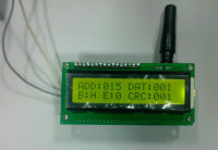
The transmitter PCB consists of a. Linx Technology_Tx module, b.2x16 LC Display and c. PIC16F628A. The transmitter has been coded to transfer data, address, error bit, CRC and bit status either high or low. We have used microcontroller to program RF_TX & RF_RX by using PICC complier. While transferring information we enable PORTB RB0. We have programmed Manchester coding technique to transfer data. The program consideration is done by standard frame Format. The standard frame Function is used to transmit data in Manchester Code, according to IEEE 802.3 definition ("1" is "LtoH" and "0" is "HtoL"). The transmission speed is indicated by "baud_tx", either 5000bps or 2500bps. It is converted into time (half period time) and stored in "semiperiod" by a simple "if" statement. Math calculations have been avoided to preserve the microcontroller's memory. The full routine sends 20 "1’s" followed by "0’s" (frame synchronism),then 8 "ADDRESS" bits, followed by "1" and "0" (byte spacer), doing the same procedure with "DATA" and "CRC" The Standard frame has been encoded and transfered to PORTB.PB0 pin. We have used LC display in order to display encoded information like address, data and CRC. Here we use continues transmission of standard data frame which can consist data, address and Bit status which we can viwe LCD screen.
Receiver Testing Procedure:
The Receiver PCB consists of linx Technology_Rx module, 2x16 LC Display and PIC16F628A. The receiver has been coded to receive data, address, error bit, CRC and bit status either high or low. We have used microcontroller to program RF_RX by using PICC complier. While receiving information we enable interrupt (ISR) of PORTB RB0. We have programmed as Manchester decoding technique to receive data. The program consideration is done by standard frame Format. The receiver PCB Module will display information after interrupt is enabled after which it display data, address and CRC on 2x16 LCD screen. We have mounted RED LED in order to identify that information has been received from the transmitter. If the receiver does not receive any data LCD screen shows Error is “1” and Bit status is “L”. Whenever the interrupt is enabled Receiver PCB module receives data and displays the frame on LCD screen.
The user may do more activities here, the only restriction is that the interrupts must be enabled; some activities, like showing data on a character LCD may disable interrupts, hence these kind of jobs must be programmed inside the ISR, after the information is received and validated and control any application as user needs.
Discussion (3 comments)