
Silicon Vacuum Tubes
on
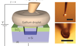
Researchers at the University of Pittsburgh have developed a semiconductor device with a vacuum channel etched in silicon for electron transport, instead of a conventional solid-state channel. This represents a return to vacuum tube technology, but on a much smaller scale.
Fast electronic devices need on short carrier transport times, which are usually achieved by decreasing the channel length and/or increasing the carrier velocity. In an ideal device, carrier motion is ballistic with no collisions, but it is difficult to achieve ballistic transport in a solid-state medium because the high electric field used to increase the carrier velocity also increases scattering. Vacuum is an ideal medium for ballistic transport, but vacuum devices typically have low emission currents and high operating voltages.
The researchers decided to combine the strengths of vacuum and solid-state technologies. They fabricated a low-voltage field effect transistor with a vertical vacuum channel etched into a metal-oxide semiconductor substrate. With a channel length of approximately 20 nm, they measured a transconductance of 20 nS/µm, an on/off ratio of 500 and a turn-on gate voltage of 0.5 V under ambient conditions. Coulombic repulsion in the electron sheet at the interface between the oxide and the metal or the semiconductor reduces the energy barrier for electron emission, leading to a high emission current density of approximately 10 μA/cm² with a bias of just 1 V.
Discussion (0 comments)