
The World's Largest FPGA
August 27, 2019
on
on
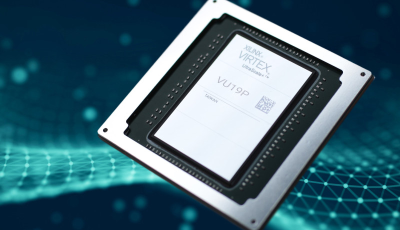
Xilinx has announced what it claims to be the world's largest FPGA device. With a total of 35 billion transistors, the VU19P offers the highest logic density and I/O number of any single device ever manufactured. It enables the emulation and prototyping of even very powerful and complex ASICs and SoCs, for example in the fields of testing and measurement, video processing, artificial intelligence and aviation.
With its 9 million system logic cells, the VU19P, which is manufactured in a 16 nm process, sets new standards for FPGAs. It offers up to 1.5 terabits per second of DDR4 memory bandwidth and up to 4.5 terabits per second of transceiver bandwidth, as well as more than 2,000 user I/Os. To picture the size of the FPGA: the chip "fits" 16 ARM Cortex-A9 CPUs. The device is 1.6 times larger than its predecessor, the industry's largest FPGA device to date: the 20-nm Virtex UltraScale 440.
The VU19P is supported and accompanied by an extensive set of debug and visibility tools and IP. The FPGA will be generally available from autumn 2020.
Read full article
Hide full article
Discussion (0 comments)