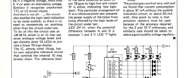
| elektor july/august 1983 94 1~ C. Bajeux 5 V logic tester The full title for the description of this circuit should be "3 state 5 V logic te...

More about logic (150)
€5 (FREE for Members)
€5 (FREE for Members)
| The circuit diagram shows perfectly clearly that T1 together with R3, R4, D5 and D6 constitute a current source for LEDs D3 and D4. As a res...
€5 (FREE for Members)
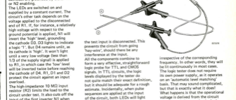
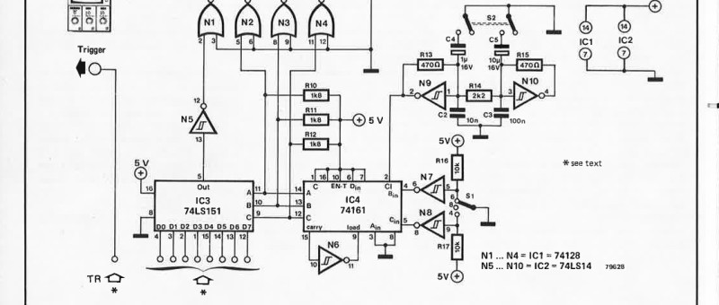
| By connecting this auxiliary circuit, the Junior Computer can be run in single cycle mode. As opposed to single step operation, where a whol...
€5 (FREE for Members)
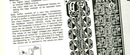
| 7.36 eiektor juiy/sugust 1981 35 input buffers for the logic analyser The input buffers described here give the logic analyser (Elektors 71,...
€5 (FREE for Members)

| 5-26 - elektor may 1981 With any project as complex as the logic analyser, the performance of the completed instrument depends to a very lar...
€5 (FREE for Members)
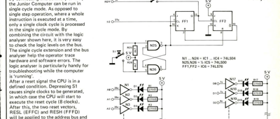
| 4-22 — elektor april 1981 logic analyser II logfr Last month, the basic principles of the logic analyser were explained with the aid of bl...
€5 (FREE for Members)
| 3-18 — elektor march 1981 logic analyser Readers who work with digital circuits regularly, and especially with micro- processors, know tha...
€5 (FREE for Members)
| 6-30 — elektor june 1980 variable logic gate For those readers who are not familiar with digital technology and thinking, a variable logic...
€5 (FREE for Members)
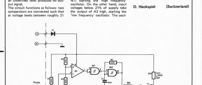
| The following circuit will provide an audible indication of CMOS logic states. Logic `O` is represented by a low frequency tone (roughly 200...
€5 (FREE for Members)
| An annoying disadvantage of fluor-escent lamps compared to the incandescent variety is the flickering delay before they actually burst into...