From simple transistors to complex systems, this article explains the building blocks of digital logic design. Learn how these powerful components work in parallel to process information at incredible speeds.
Digital logic designs do truly amazing things. They can implement complex state machines with latency of only a few nanoseconds. They can perform parallel digital signal processing at rates of multiple DVD movies per second. They can electrically interconnect simple semiconductor chips into an advanced circuit. Unlike CPUs, digital logic designs can do everything in parallel (all tasks at the same time) rather than sequentially (one task after the other).
CMOS Transistor Theory 101
The MOSFET (“metal-oxide-Semiconductor Field-effect transistor”) is the building block of modern digital chip designs. Its long history began with a patent filed by Austro-Hungarian born physicist Julius Edgar Lilienfeld in 1925 for a device that used an electric field to control current. William Shockley and others further developed the concept which eventually led to a working Junction Field-Effect Transistor (JFET) in the 1950s. In 1955, Lincoln Derrick and Carl Frosch grew a silicon dioxide layer over a silicon wafer and observed surface passivation effects. This discovery led to the MOSFET transistor being invented by Mohamed Atalla and Dawon Kahng at Bell Labs in 1959.
Note: JFETs are still used in low-noise analog applications, while MOSFETs dominate the digital world.
By combining two types of MOSFET transistors (P and N), a CMOS gate is formed. MOSFETs rule the modern digital world as they are small, easy to manufacture, fast, and very low power. It is estimated that more than 20 trillion MOSFETs are manufactured every second.
Figure 1: MOSFET Transistor
To create a MOSFET transistor, you start with a silicon wafer and dope regions to create two small n+ regions that surround the wafer’s default p- region. SiO2 (typically) is deposited above that NPN region to form a very thin gate oxide insulator. Connect some metal to the two n+ regions, the substrate body, and the gate oxide, and you have a MOSFET transistor. Modern MOSFETs primarily use a conductive polysilicon connector to the gate oxide. Maybe they should be called PSOSFETs instead!
Here’s the thing about silicon: Silicon is a chemical element (Si) on the periodic table. By itself, silicon is not a very good conductor. By adding (doping) a small amount of an element like phosphorus or boron—which are similar to silicon but have an extra or missing valence electron—things get really interesting. The doping process creates an imbalance in the number of electrons and holes within the crystal lattice structure, increasing conductivity. The result is a material that can function as either a strong insulator or a conductor—on demand.
I like to think of silicon like cookie dough: not very interesting by itself, but add some chocolate or butterscotch chips and BAM! You’ve made something really special.
Once the NPN-doped silicon structure is formed (as shown in the figure above), the p-type area directly beneath the gate creates the channel region, which may or may not permit electron flow.
Key Characteristics of a CMOS Gate:
Insulated Control: The gate is separated from the channel by a thin layer of silicon
dioxide (SiO2), creating a high-input impedance.
Electric Field Activation: Applying a voltage to the gate generates an electric field,
allowing current to flow between drain and source.
Capacitive Behavior: The gate behaves like a capacitor.
Electrically, the gate of the NMOS transistor looks like a capacitor. Ignoring small amounts of leakage current, the transistor’s gate only requires energy when switching to charge and discharge its capacitance. When the gate is at GND potential, no current may flow through the NMOS transistor’s channel region. When a VCC voltage is applied to the gate, an electric field is created in the channel region and current may then flow between the drain and source.
Note: Analog designers often use VDD and VSS to represent the positive supply rail and ground nodes. In this book, I use VCC and GND—different names for the same thing, much like cilantro and coriander leaves. Transistor-level designers may not appreciate this choice, but this is my book—and they’re more than welcome to write their own.
Power consumption of CMOS transistors is primarily dictated by CV2F, where:
F is the gate switching frequency.
C is the gate capacitance (including parasitic wiring).
V2 is the square of the voltage applied to the gate.
As Moore’s Law continues to shrink transistors, both V and C decrease, leading to lower power consumption and higher switching speeds.
The “C” in “CMOS” stands for “Complementary”. MOSFETs come in complementary pairs called NMOS and PMOS. The NMOS transistor is built from the NPN structure described above, and is used to sink current on its Drain to a Source connected to GND. The PMOS transistor is the inverse. Built from a PNP structure, it is used to source VCC current from its Source node to its Drain node. The NMOS is turned “ON” by applying VCC to its Gate node. The PMOS is turned “ON” by applying GND to its Gate node.
Note: The terms PFET (P-channel Field-Effect Transistor) and NFET (N-channel Field-Effect Transistor) are also commonly used to refer to PMOS (P-channel MOSFET) and NMOS (N-channel MOSFET) transistors.
Figure 2: Complementary NMOS and PMOS Transistors
When I think of MOSFET transistors, I like to think of three cookies in a row: chocolate chip, butterscotch chip, and chocolate chip. You turn the cookie channel on by dumping a bag of chocolate chips (excess electrons) next to the butterscotch chip cookie (at the Gate). Every butterscotch chip gets displaced by the chocolate chips from the bag, and now you have three chocolate chip cookies in a row (and the current flows). Anyone else hungry now?
Tip: It’s important to connect only digital signals to the digital input of a CMOS device. Connecting an analog signal to a digital input risks Simultaneous Conduction, a CMOS state where both NMOS and PMOS transistors conduct simultaneously, creating a resistive short circuit between VCC and GND. Picture a teeny-tiny Edison incandescent bulb inside your chip. This not only wastes power but also risks damaging the transistors due to overheating. Instead, use an analog comparator, and always follow the Vil and Vih specifications for a CMOS input to prevent this condition. Your tiny little CMOS transistors will thank you. Ignoring CMOS simultaneous conduction poses a serious risk to long-term system reliability.
For whatever reason, there is no universally agreed upon symbol set for NMOS and PMOS transistors. The figure above is just one of many that you may see in literature. For this reason, I will create my own to use in this chapter, as I think it conveys some important information. Also, this is my book—and no one can stop me.
Figure 3: CMOS simplified “Switch” symbols
NMOS Symbol Information:
Gate turns the channel on with a high(VCC) signal.
PMOS Symbol Information:
Gate turns the channel on with a low(GND) signal.
The NMOS and PMOS can be thought of as Gate-controlled switches that have a small amount of resistance in series with their switch. Drawing a CMOS inverter using modified NMOS and PMOS symbols illustrates the simplicity of building CMOS gates out of MOSFET transistors. This configuration is known as a CMOS totem-pole structure. The arrows in the MOSFET symbols do not represent diodes; rather, they indicate the direction of current flow when the channel is formed.
Figure 4: CMOS Inverter
The manufactured inverter would look like the following in a silicon wafer side-view.
Figure 5: CMOS Inverter Layout
By adding just a few more NMOS and PMOS transistors in series and in parallel, more complicated gates like NANDs and NORs are easily created. Following them with another NMOS-PMOS pair (inverter) creates AND and OR gates.
By combining digital logic gates like ANDs and ORs, more complex logic structures—such as adders, subtractors, comparators, and multipliers—can be created. However, these advanced structures alone have limited functionality, as they lack memory. They can compute an answer but cannot store it for another logic block to use. To achieve this, a digital storage element is required.
D-Type Flip-Flop
The D Flip-Flop is the primary building block of digital logic design. As a digital logic design deals with binary bits, the simple D Flip-Flop is the keeper of those bits. The smallest D Flip-Flop I have come across was made with twenty NMOS and PMOS transistors. You don’t need to know how it works, but you should know that those transistors are there. The eight transistors with clocks on their gates are especially important.
Figure 7: D-Type Flip-Flop
It’s extremely easy for an RTL designer to forget about the CMOS transistor structure of a D Flip-Flop. However, it’s important not to. It may also be tempting to assume that a flip-flop with static input and output isn’t consuming much power. That assumption would be incorrect. The eight transistor gates driven by a clock represent eight capacitive loads, which, at CV²F, account for a significant portion of total power consumption in CMOS digital logic. In my experience, CMOS clock trees within a chip typically consume about one-third of the device’s total power.
Figure 8: CMOS D-Type Flip-Flop in transistors
Tip: To conserve power in a digital logic design, enable the clock to a flip-flop only when necessary. When the clock is gated, the Q output retains its logic state, and the flip-flop’s power consumption is reduced to nearly zero.
Pipelining, or adding flip-flops between combinatorial logic stages, is an important aspect of digital logic design for meeting timing. However, pipelining is not free, as it incurs a significant cost in both area and power. A good digital designer knows how to pipeline a design just enough to meet timing, but not so much that it needlessly consumes excessive area and power.
The Intel Pentium 4 is a classic example of over-pipelining a design. The 1990s saw 80x86 architecture rapidly go from 100 MHz to 1 GHz FMAX CPU designs. Intel’s performance desktop CPU plan for the 2000s was to then go from 1 GHz to 10 GHz. This plan resulted in the NetBurst microarchitecture, which more than doubled the traditional 80x86 pipelining. In the end, the Pentium 4 topped out at 3.8 GHz, and Intel abandoned NetBurst and backtracked to the much lower power Pentium M (Mobile) architecture initially intended only for laptops.
With CMOS clock frequencies reaching a ceiling of around 5 GHz, the industry’s focus has shifted to parallel processing, now fueling the rise of GPUs in AI. Meanwhile, FPGAs play a crucial role in parallel computing, offering significant growth potential for massively parallel signal processing.
More on Digital Logic Design
For more information about digital logic design, refer to Kevin Hubbard's book, Mastering FPGA CHip Design(Elektor 2025), from which this article (Ch. 1) is sourced.
Subscribe
Tag alert: Subscribe to the tag Circuits & Circuit Design and you will receive an e-mail as soon as a new item about it is published on our website!



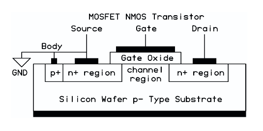
 Once the NPN-doped silicon structure is formed (as shown in the figure above), the p-type area directly beneath the gate creates the channel region, which may or may not permit electron flow.
 Key Characteristics of a CMOS Gate:


Discussion (1 comment)