
Multi-Channel Power Analyzer
on
When making voltage, current and power measurements on AC-powered devices things are getting more complicated than measuring DC, because waveform and phase-shift between voltage and current play an important role here. This instrument not only measures and calculates quantities, but also shows waveforms and spectra of AC-signals on a graphical LCD.
This project was inspired by the AC/DC Power Meter published in Elektor Magazine in September 2015. At first I thought it was very interesting and I wanted to build one myself, but I found some limitations and drawbacks in this design, so I decided to develop an “improved” design. Things I wanted to improve were:
- The input circuit: It should be possible to measure current and voltage independently: the current through the connecting leads should not influence the voltage reading.
- The sampling rate: the low sampling rate makes it only possible to measure the first eight harmonics of a 50 Hz signal (with perfect filter). This should be increased to the first 40 harmonics.
- The range switching and offset correction must be made automatically.
This means that the input and amplifier circuit need a complete redesign. Also, a microcontroller is needed at the hot-side, to make automatic offset correction and auto-ranging possible. The block diagram in Figure 1 shows a main board and (up to) three satellite boards.

The Main board
The schematic (see Figure 2) is largely a copy of the EasyPIC V7 board, with a graphic LCD touch screen as user interface.

A square wave oscillator (circuit around IC1) generates a 12 Vpp square wave with a frequency of about 150 kHz for powering the satellite boards. The data communication with the satellite boards will be via I2C, where the microcontroller on the main board is the master and the satellite boards are the slaves.
The power supply section of the main board supports either a 12 V stabilized or a 15...18 V supply without stabilization. The selection can be made by a solder joint (SJ1). There are two other solder bridges/jumpers: MAX1 and MAX2. With these, the number of channels can be set for the master: closing MAX1 only means one, closing MAX2 means two and closing both means three channels (satellite boards). Some jumper wires (marked with Jx in schematics and on the main PCB layout) are used to avoid the need for a multilayer PCB.
The Satellite board
On the Satellite boards (schematic in Figure 3) I wanted to measure voltage and current independently.

This is not fully realizable, but with the circuit the low voltage input and the current input can float about +/- 1 V with respect to each other. This is realized by the diode D3, D4, D7, D8. Without measures taken, the circuit can be damaged by a wrong connection: the high potential to the low voltage input and also the current input at the low voltage side. To prevent this damage, the circuit with T10…T14 and reed relay K1 is added. A first current limitation is realized by R11: at 750 V input voltage the maximum current is 0.5 A. If the current through R11 is larger than some 10 to 20 mA, there will be a small current through R34, which is detected by T11 and T13. This will trigger the thyristor circuit with T10 and T12. Once triggered the thyristor circuit will remain in this state and will switch off T14 and K1. Signal OC indicates to the microcontroller that the protection is triggered. When there is no power K1 is also switched off (V-low is disconnected), so then the circuit is safe. To restore operation the power of the circuit must be disconnected and connected again.
The voltage divider gives 100 mV output at the maximum input voltage of 750 V (DC), the maximum AC voltage will be about 500 V. The voltage drop at the 6.5 mΩ current sense resistor R62 is about 100 mV at 15 A-DC (about 10 A-AC). The amplifiers for voltage and current are identical, so I’ll describe only the voltage amplifier. T1, T2 and T4, T6 serve as switches to connect the differential amplifier either with the signal from the input circuit or short the input to make offset measurement possible. The value of the offset can be stored and subtracted later from the measurement to make a “clean measurement” possible. The amplifier is a common instrumentation amplifier. T3, T5 switch the gain of the first stage to either 1x or 25x. IC5 makes the differential signal single ended. The last stage with IC4 can switch the gain to either 1x or 5x. So there can be four gains: 1x, 5x, 25x or 125x. The gain setting will be under control of the microcontroller IC13. The amplifier will generate a positive or negative signal with respect to COMV. This signal is 0.5 times VREF, which is generated by the circuit around IC3. VREF is 4.5 V, so COMV, COMI and CINV are 2.25 V. VREF and CINV are connected to the ADC of the PIC-controller. The ADC of the PIC18F26K80 used here can convert to 13 bits when used in the indicated way (12 bits plus a sign bit). For 750 V this gives a resolution of about 200 mV per bit. For 6 V about 1.6 mV/bit. I consider this as sufficient for this purpose.
The I2C address of a satellite board is programmed by closing or opening SJ1 and SJ2 on the board. Closing SJ1 makes the board channel 1, closing SJ2 makes it channel 2 and closing both solder joints makes it channel 3.
Galvanic isolation
The square wave coming from the main board is fed to the transformer at the right (ratio 1:1). The rectifiers give then an output voltage of something less than 6 V. With parallel regulators this is controlled to +/- 5 V. The windings of the transformer have an isolation value of 900 V, so the total isolation will be 1800 V peak, provided that the rest of the construction is OK. The I2C signal will go via IC14, which has an isolation value of 4 kV peak. So the satellite boards will be completely floating with respect to the main board and with respect to each other.
Update of the satellite board circuit
After the first prototype was built, tests proved that some corrections had to be made. The crosstalk from the switching signal to the measurement signal in the offset switches had to be limited. Therefore C41-R102 and C40-R103 are added. The protection circuit reacted on spikes, for example when a test lead was plugged. The sensitivity for spikes has been decreased by adding C33. D14 and R101 also limit he sensitivity for positive signals.
When the amplifiers have the highest gain (approximately 2750x), an offset control is needed. This control is switched off when the gain is lower. Depending the sign of the offset a selection has to be made with the solder jumper.
Unfortunately I forgot some decoupling capacitors in the supply part, these had to be added too. The part list for this project in Open Office format can be downloaded from [2]. Order codes for Farnell are given, but of course you can choose any supplier.
Software for the satellite board
The program is written in mikroBasic for PIC (V5.6.1) from MikroElektronika, a programming language that is relatively easy to understand.
I wanted that a frequency range from (a bit) less than 50 Hz to a few hundreds of Hz could be processed. Therefore, the signal needed to be sampled for at least 30 ms. Then, at 50 Hz there are at least three zero-crossings, so you can detect one period. But that is only true when these zero-crossings are equidistant. With a duty cycle unequal to 50 % at 50 Hz, 30 ms is not sufficient, that’s why I have chosen for 35 ms. Then with a duty-cycle of less than 25 % there it is possible that the frequency is not correctly determined at 50 Hz, with higher frequencies there is no problem. Signals with less than three zero-crossings during the sampling period are treated as DC.
The second question is how many samples will be taken in these 35 ms. A sampling frequency of 10 kHz or higher would be ideal. I have chosen for 357 samples at 10.2 ks/s. This leads to a integer multiple of samples for 50 and 60 Hz signals. These frequencies can then be analyzed with the highest accuracy.
There is a library with I2C commands in mikroBasic, but these are only for an I2C master. For an I2C-slave I had to write my own procedures. These procedures are needed to setup and control the communication with the main board, the I2C master. The latter just requests and displays information from the satellite boards, (auto-) ranging and offset, all signal processing, including sampling and filtering is performed on the satellite board(s).
Fast Fourier transforms are also calculated on the satellite boards. The calculations are not invented by me but “borrowed” from [3]. Digital filtering is based on chapter 16 of The Scientist and Engineer's Guide to Digital Signal Processing. A Blackman-window is used and the filter has 13 coefficients (M=12). The choice of the length of the filter is a compromise between calculation time, memory needed and performance (i.e., suppression of signals above 2.55 kHz and attenuation of signals below 2.55 kHz).
Assembly
A front panel has been designed (for a three channel version), which can be ordered at Schaeffer’s. I used a metal case (order code 1510827 at Farnell, manufacturer Metcase, M5503110).
Figure 4 shows some detailed pictures of the hardware in this enclosure, giving an impression of what the Power Meter can look like and how the units are fixed in the case. Note the ready-made, standard power supply that is used to power the Power Analyzer.
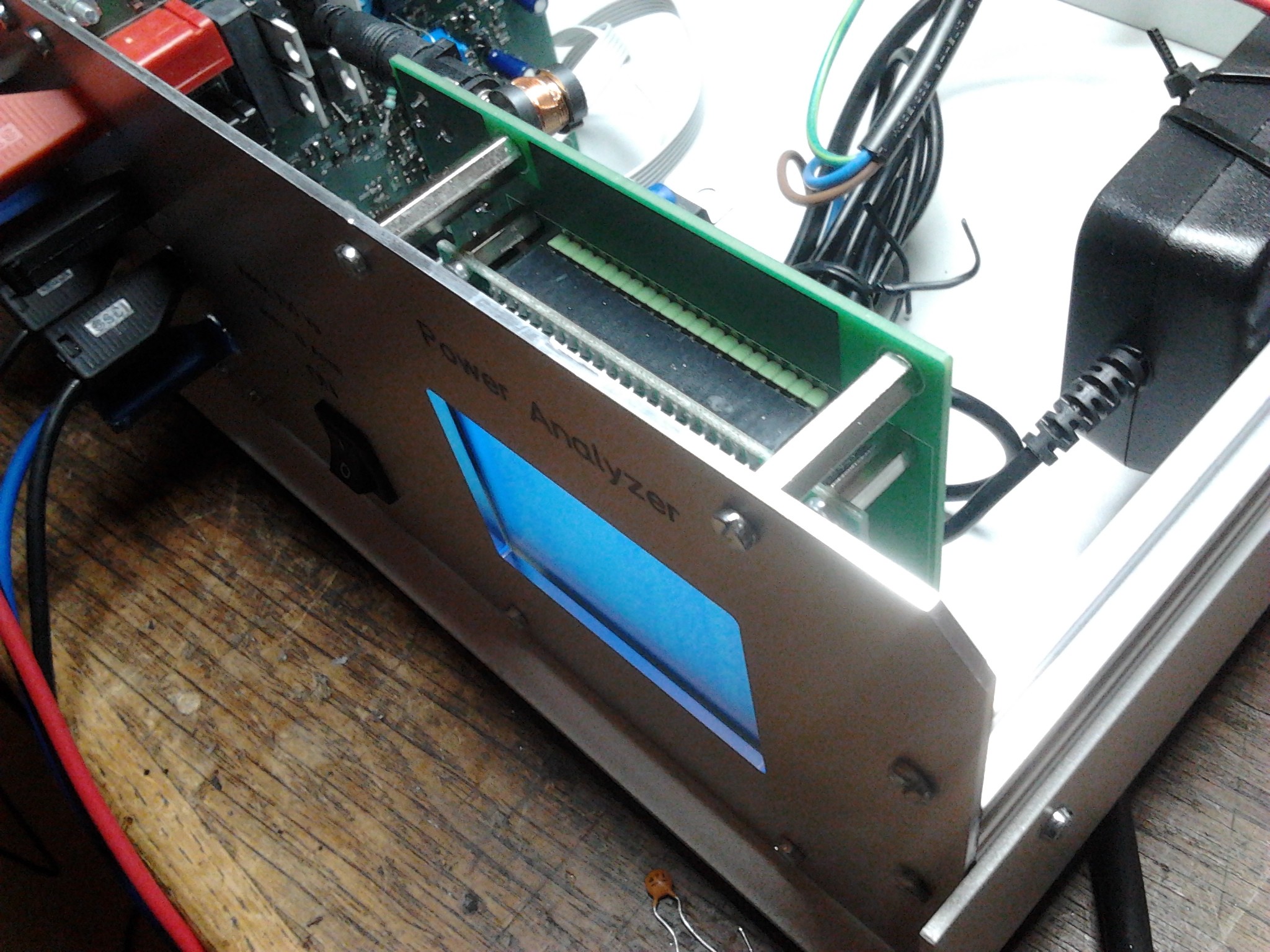

Figure 4c shows one of two extra brackets, which are added to prevent the front panel from bending when test leads are plugged in or out.

An extra hole in the top and bottom cover must be drilled to attach the brackets. I used a metal housing so the enclosure must be connected to the mains Protective Earth, see Figure 4d.

Operation
After switching on, the measurement screen appears. It displays some units and their values for the channel that is selected. At the top of the screen you can select other channels (if available).
The screen can display a maximum of seven measurement values, selected in the Configuration Screen.
First go to the Main Menu (top right of the screen). Choose Configuration and then the Configuration Screen will appear with 16 values to choose from. The selected values to be displayed will be highlighted.
Some of these values will go without saying, but some need explanation. Vdis and Idis (distortion) are calculated using:
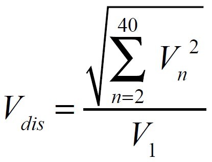
where VN stands for the amplitude of harmonic N of the signal.
Re-P means real power, P-VA means Vrms x Irms, Im-P means imaginary power, and PF means power factor, i.e. Re-P / P-VA.
If you choose Eff-> you enter the Efficiency Screen. Here you can choose the formula which describes the power relation that you are investigating and then you go back to the Configuration Screen. If you go back to the Measurement Screen, the chosen formula with the calculated value is displayed for all channels.
Back in the Configuration Screen you can also choose for Graphs-> Pressing this you can choose between Scope or FFT. Press Scope. This brings you to select traces. Trace1 will always be displayed. A selected trace will be high-lighted. All traces can be “connected” to a channel and to V, I or P of that channel. The display will be “triggered” by a positive zero crossing of Trace1. The display will give you an impression of the wave shape of the signals and their phase relation. Two periods of the signal will be displayed. The amplitude of the signals is always the same: voltage signals have the maximum amplitude. To distinguish them from voltage signals, current signals are displayed with a 80 % and power signals at 60 % amplitude. See for example the waveforms of a transformer which goes in saturation in Figure 6.

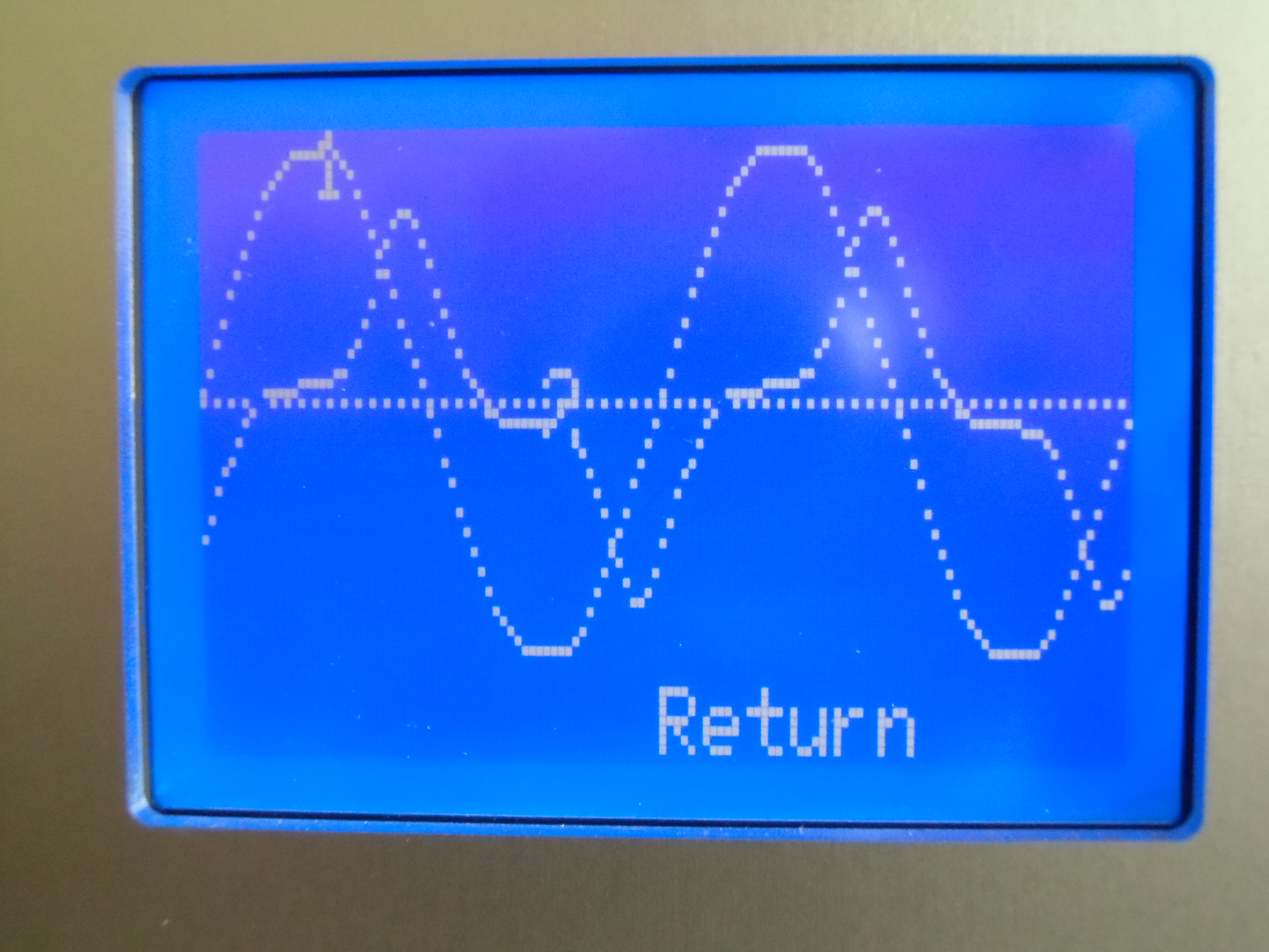
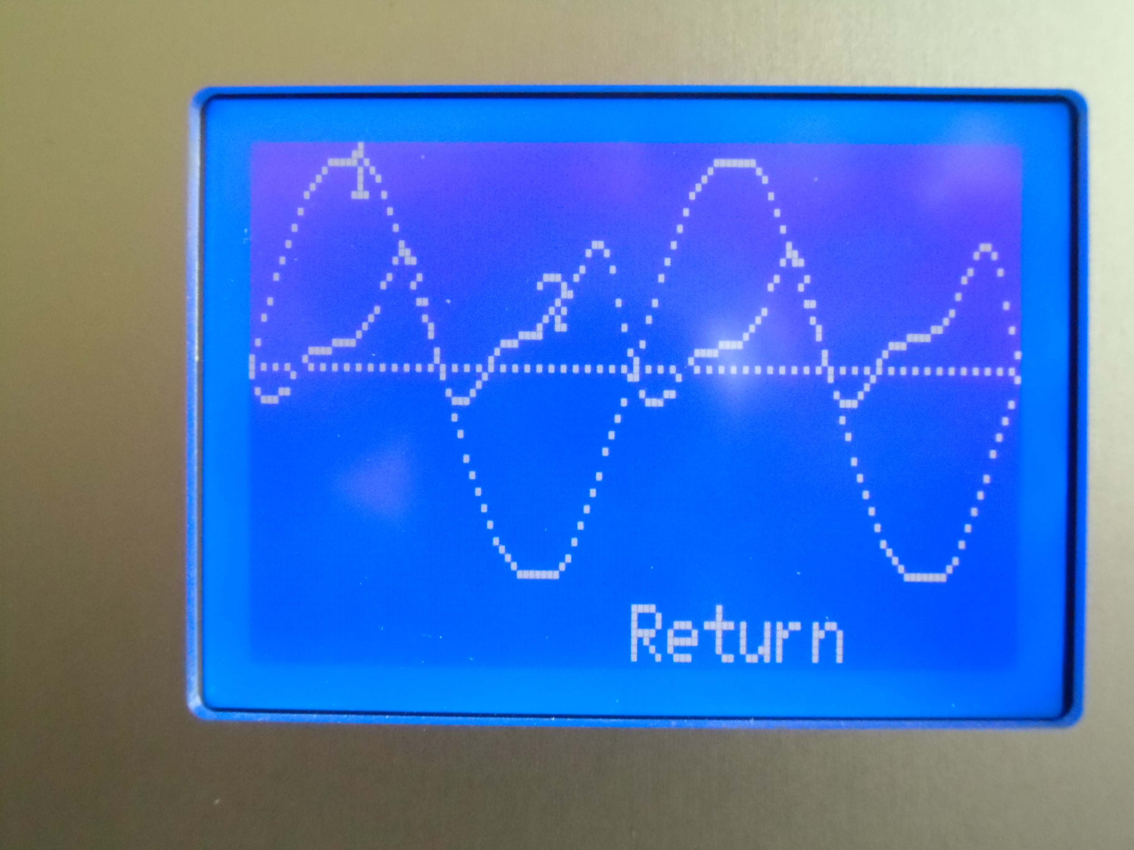
The scope display doesn’t show absolute values, it’s just an indication of shape and phase relation.
Back in the Graphic Screen, press FFT. This shows the FFT components of a selected signal. On top of the screen you can select the channel, LINear or LOGarithmic display and either V or I. The largest harmonic (usually but not necessarily the first harmonic) is displayed at 100 % or 0 dB. The horizontal scale gives the number of the harmonics, not its frequency.
When entering the Logging feature, you must first select the time period that you want to apply. Possible values are between 0.25 h and 128 h in steps of a factor of 2. Next step is to select how many traces you want to log (maximum three). Each trace can be linked to a channel and from that channel you can choose either V, I or P. Pressing Continue immediately starts the logging. An alphanumeric screen will be shown, where you can watch the average, maximum and minimum value and the elapsed time. You can also go to the graphical screen. At the top of the screen you can select another trace, if it is switched on. Pressing Return brings you back in the main screen, the collected data are lost.
You can select Crest factor (V-CF or I-CF) in the configuration screen. It simply divides the highest peak value (positive or negative) by the RMS-value of the signal. Remember that the bandwidth of the measuring amplifiers is 2.5 kHz, so this function is not suitable for audio. Only until, say 250 Hz depending on your taste.
How to calibrate and adjust
From the Main Screen you can go to the Calibration screen. You can choose between calibrating the touchscreen and calibrating the channels. At the first start up the touchscreen calibration procedure will automatically be presented. Use a pencil or wooden stylus to calibrate (and use) the touch screen.
In the channel calibration you will first be prompted to select a channel. Then the software enters a screen where voltage, current and frequency can be measured and adjusted. In this screen the automatic ranging for V and I is disabled, which will make it easy to adjust the calibration for each range. With the arrows (< and >) you can change ranges and adjust the measured value.
The best method to adjust the frequency is to connect a digital oscilloscope to TP8 (signal) and TP2 (GND) on the satellite board of the selected channel. Adjust the visible pulse width to 35.00 ms with the arrows on the frequency line. Second best method to adjust the frequency is to use a signal source with a calibrated frequency of 50 or 60 Hz and adjust the reading to 50.00 or 60.00 Hz. The reading can vary ±0.5 %.
When done calibrating a channel, press ->OK. Then the calibration data are stored on the satellite board of the selected channel.
As far as I’m concerned this project is finished, there will be no more large additions or changes. But of course, I will answer any question.
This article is based on the information presented on the Elektor Labs project page at [2]. On this page, more detailed information on this Power Analyzer including software, PCB design files and BOM can be found or downloaded. The Eagle CAD-files on Elektor Labs are up to date with the most recent changes, but newer versions of the PCBs have not been built and/or tested!
[190133]
Questions or comments?
Do you have questions or comments about his article? Email the author at w.j.dijkman@onsbrabantnet.nl or contact Elektor at editor@elektor.comBuilding the transformer
Transformer TR1 is home made. Here is the recipe.Ingredients (mentioned at the bottom of the parts list): two core halves, two clips, one coil former, all for EF20, wire with 900 V isolation and diameter of max 1.3 mm.
Take the coil former and cut off pins 2, 3, 4, 7, 8 and 9.
With the wire make 9 turns between pin 1 and 10. You shall exactly fill one layer.
Repeat to make 9 turns between pins 5 and 6. Again you shall exactly fill one layer.
Put in the core halves and put on the clips. There is no air gap.
If everything went well, you will have a transformer with an equal primary and secondary inductance of about 125 μH. Capacitance between primary and secondary will be in the range of 30 pF.
How to connect
There is a difference between connecting test leads for measuring the power consumption of a load or measuring the power supplied by a source, as can be seen in Figure 5.

With the indicated methods the voltage drop of the connection leads and the current measurement section is eliminated. The voltage difference between the I connections and the V- connection must remain below 0.5 V. Otherwise the protection circuit is triggered, and the power supply has to be cycled.
Streamers:
WARNING. Working with high voltage can be fatal. The circuit described here is not for beginners. Do not build or use it unless you are experienced in dealing with high voltages!
Want more great Elektor content like this?
Take out an Elektor membership today and never miss an article, project, or tutorial.
Discussion (5 comments)