
Power Analyzer
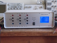
1, 2 or 3 channel power analyzer, giving number or graphic display (scope picture or FFT) on a 128 x 64 LCD
This project was inspired by the Power Meter published in Elektor Magazine in September 2015. At first sight I thought it was very interesting and I wanted to make one myself. But reading further on I found some limitations and drawbacks. So in the end I decided to start with an "improved" design.
Things I wanted to improve were:
The above means that the input and amplifier circuit need a big redesign. Also a uP is needed at the hot-side, to make the offset correction and auto-ranging possible.
The Main board is not very original. The idea is to use a 128 x 64 GLCD as used in the EasyPIC7 development board for display and for control I use also the touch panel. So the biggest part of the main board is a copy of the circuits of the EasyPIC7 board. On top of the circuit diagram there is a square wave oscillator, which generates a square wave of 12 Vpp at a frequency of about 150 kHz. This signal is used to power the Satellite boards. The communication with the Satellite boards will be via I2C. The uP on the main board will be the master, the satellite boards are the slaves. The connectors to the satellite boards are at the right of the diagram.
The Satellite boards deviate a lot from the original in Elektor. I start with the input circuit, at the far left. I wanted to measure voltage and current independently. This is not fully realizable, but with the given circuit the low voltage input and het current input can float about +/- 1 V with respect to each other. This is realized by the diode D3, D4, D7, D8. Without measures taken, the circuit can be blown up by a wrong connection: the high potential to the low voltage input and also the current input at the low voltage side.
To prevent damage the circuit with T10 …T14 and reed relay K1 is added. A first current limitation is realized by R11: at 750 V input voltage the maximum current is 0.5 A. If the current through R11 is larger than some 10 to 20 mA, there will be a small current through R34, which is detected by T11 and T13. This will trigger the thyristor circuit with T10 and T12. Once triggered the thysistor circuit will remain in this state and it will switch off T14 and K1. Signal OC indicates to the uP that the protection has been triggered.
When there is no power K1 is also switched off (V-low is disconnected), so then the circuit is safe.
To restore operation the power of the circuit has to be disconnected and connected again.
The voltage divider gives 100 mV output at the maximum input voltage of 750 V (DC).
The maximum AC voltage will be about 500 V.
The current sense resistor is now 6.5 mΩ to give about 100 mV at 15 A-DC (about 10 A-AC).
The amplifiers for voltage and current are equal. I describe only the voltage amplifier (on top). T1, T2 and T4, T6 form switches which connect the differential amplifier either with the signal from the input circuit or short the input to make offset measurement possible. The value of the offset can be stored and subtracted later from the measurement to make a “clean measurement” possible.
The amplifier is a common instrumentation amplifier. T3, T5 switch the gain of the first stage to either 1x or 25x. IC5 makes the differential signal single ended. The last stage with IC4 can switch the gain to either 1x or 5x. So there can be four gains: 1x, 5x, 25x or 125x. The gain setting will be under control of the uP. The amplifier will generate a positive or negative signal with respect to COMV. This signal is 0.5 times VREF, which is generated by the circuit on the top right of the circuit diagram. VREF is 4.5 V, so COMV, COMI and CINV are 2.25 V. VREF and CINV are connected to the ADC of the uP. The ADC of the used PIC18F26K80 can convert to 13 bits when used in the indicated way (12 bits plus a sign bit). For 750 V this gives a resolution of about 200 mV / bit. For 6 V about 1.6 mV/ bit. I consider this as sufficient for this purpose.
Before sampling, the signal needs to be filtered, the cut-off frequency has to be 2.4 kHz. The roll off is maybe an issue. I have chosen for a combination of four first-order filters. When calculated for 3 dB attenuation at 2.4 kHz the attenuation at 5 kHz is only 0.32 (about – 10 dB). It is questionable whether this is sufficient.
The square wave coming from the main board is fed to the transformer at the right (ratio 1:1). The rectifiers give then an output voltage of something less than 6 V. With parallel regulators this is controlled to +/- 5 V.
The windings of the transformer have an isolation value of 900 V, so the total isolation will be 1800 V peak, provided that the rest of the construction is OK. The I2C signal will go via IC14, which has an isolation value of 4 kV peak. So the satellite board will be completely floating with respect to the main board and with respect to each other.
So far about the circuit diagrams. I now have to write some software
Things I wanted to improve were:
- The input circuit: It should be possible to measure current and voltage independently from each other: the current through the connecting leads shall not influence the voltage reading.
- The sampling rate: the low sampling rate makes it only possible to measure the first 8 harmonics of a 50 Hz signal (with perfect filter). This should be increased to the first 40 harmonics.
- Range switching: The used method was a bit clumsy and also risky: Suppose that you are measuring at a 230 V circuit and has to make a quick adaptation... The range switching shall be made automatic.
- Offset correction: this shall also be automatic.
The above means that the input and amplifier circuit need a big redesign. Also a uP is needed at the hot-side, to make the offset correction and auto-ranging possible.
2016-06-09
The intended block diagram is given in the drawing at the top of this document. There will be a main board and three satellite boards. The preliminary circuit diagrams are given in the attachments. At the moment of writing, nothing has been tested yet.The Main board is not very original. The idea is to use a 128 x 64 GLCD as used in the EasyPIC7 development board for display and for control I use also the touch panel. So the biggest part of the main board is a copy of the circuits of the EasyPIC7 board. On top of the circuit diagram there is a square wave oscillator, which generates a square wave of 12 Vpp at a frequency of about 150 kHz. This signal is used to power the Satellite boards. The communication with the Satellite boards will be via I2C. The uP on the main board will be the master, the satellite boards are the slaves. The connectors to the satellite boards are at the right of the diagram.
The Satellite boards deviate a lot from the original in Elektor. I start with the input circuit, at the far left. I wanted to measure voltage and current independently. This is not fully realizable, but with the given circuit the low voltage input and het current input can float about +/- 1 V with respect to each other. This is realized by the diode D3, D4, D7, D8. Without measures taken, the circuit can be blown up by a wrong connection: the high potential to the low voltage input and also the current input at the low voltage side.
To prevent damage the circuit with T10 …T14 and reed relay K1 is added. A first current limitation is realized by R11: at 750 V input voltage the maximum current is 0.5 A. If the current through R11 is larger than some 10 to 20 mA, there will be a small current through R34, which is detected by T11 and T13. This will trigger the thyristor circuit with T10 and T12. Once triggered the thysistor circuit will remain in this state and it will switch off T14 and K1. Signal OC indicates to the uP that the protection has been triggered.
When there is no power K1 is also switched off (V-low is disconnected), so then the circuit is safe.
To restore operation the power of the circuit has to be disconnected and connected again.
The voltage divider gives 100 mV output at the maximum input voltage of 750 V (DC).
The maximum AC voltage will be about 500 V.
The current sense resistor is now 6.5 mΩ to give about 100 mV at 15 A-DC (about 10 A-AC).
The amplifiers for voltage and current are equal. I describe only the voltage amplifier (on top). T1, T2 and T4, T6 form switches which connect the differential amplifier either with the signal from the input circuit or short the input to make offset measurement possible. The value of the offset can be stored and subtracted later from the measurement to make a “clean measurement” possible.
The amplifier is a common instrumentation amplifier. T3, T5 switch the gain of the first stage to either 1x or 25x. IC5 makes the differential signal single ended. The last stage with IC4 can switch the gain to either 1x or 5x. So there can be four gains: 1x, 5x, 25x or 125x. The gain setting will be under control of the uP. The amplifier will generate a positive or negative signal with respect to COMV. This signal is 0.5 times VREF, which is generated by the circuit on the top right of the circuit diagram. VREF is 4.5 V, so COMV, COMI and CINV are 2.25 V. VREF and CINV are connected to the ADC of the uP. The ADC of the used PIC18F26K80 can convert to 13 bits when used in the indicated way (12 bits plus a sign bit). For 750 V this gives a resolution of about 200 mV / bit. For 6 V about 1.6 mV/ bit. I consider this as sufficient for this purpose.
On the sampling rate and filtering
I want to measure the first 40 harmonics from a 50 or 60 Hz signal. So the highest frequency is 2.4 kHz. The minimum sampling rate has then to be 4.8 ks/s, but 7.5 or 10 ks/s is better. The uP has then to make 15 or 20 20ks/s (for voltage and current). The PIC18F26K80 needs a minimum of 17 µs for one conversion, so a maximum speed of 58 ks/s is possible. (forgetting the time needed to work with the acquired data). So the speed does not seem an issue.Before sampling, the signal needs to be filtered, the cut-off frequency has to be 2.4 kHz. The roll off is maybe an issue. I have chosen for a combination of four first-order filters. When calculated for 3 dB attenuation at 2.4 kHz the attenuation at 5 kHz is only 0.32 (about – 10 dB). It is questionable whether this is sufficient.
The square wave coming from the main board is fed to the transformer at the right (ratio 1:1). The rectifiers give then an output voltage of something less than 6 V. With parallel regulators this is controlled to +/- 5 V.
The windings of the transformer have an isolation value of 900 V, so the total isolation will be 1800 V peak, provided that the rest of the construction is OK. The I2C signal will go via IC14, which has an isolation value of 4 kV peak. So the satellite board will be completely floating with respect to the main board and with respect to each other.
So far about the circuit diagrams. I now have to write some software
Updates from the author