
Universal Triac Control Module with ATmega
on

Everyone involved in electronics knows more or less what thyristors and triacs are, how they work and how they are used. However, these components offer so many possibilities that only specialists are able to fully exploit their potential. Nowadays thyristors are mainly used in special applications with high voltages (above 1 kV) and strong currents (many kiloampères), so this article only focuses on triacs.
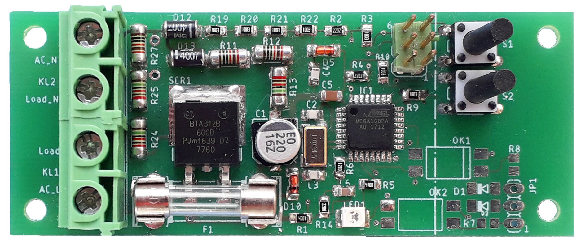
First we look at the basic operation of triacs and the relevant parameters. Then we describe the circuitry of the control module. Figure 1 shows the author’s finished prototype. Many functions are possible with this combination of an ATmega microcontroller and a triac. Depending on the firmware, the module can be used as a simple switch or remote switch, a timer, a dimmer, or a soft-start module for switching inductive loads such as transformers or motors.
Basics
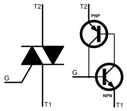
A triac is a semiconductor switch that conducts current in both directions when it is switched on, which means it is an AC switch. The load current flows through the two electrodes T1 and T2 (here ‘T’ stands for ‘terminal’). These electrodes are also designated MT1 and MT2 (for ‘main terminal’), and in the past they were also called A1 and A2 (for ‘anode’). The third electrode is the gate (G), which is the control lead. Figure 2 shows the Elektor circuit diagram symbol for a triac (on the left) and a simple equivalent circuit (on the right).
and an equivalent circuit for the first quadrant,
composed of PNP and NPN transistors (right).
A triac remains in the off state until the current flowing from the gate (G) to T1 is high enough to switch it on. Once the triac is switched on, it remains in the on state until the current between T1 and T2 drops below a threshold value, which depends on the type. Then it returns to the off state. In operation with an AC voltage, this means it switches off at every zero crossing of the current, which is not necessarily in phase with the voltage, unless it is constantly kept on by the gate current. Accordingly, a triac can be triggered by a short, low-energy pulse on the gate, but it cannot be directly forced to switch off.
T1 is the reference point (reference voltage) for the gate G. There are four different directions of current flow, depending on the polarity of the voltages on the gate and T2 relative to T1. These are shown by the four-quadrant diagram in Figure 3.
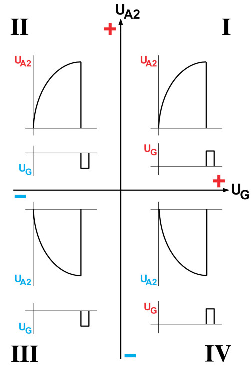
The X axis represents the polarity of the voltage on the gate relative to T1. The Y axis represents the polarity of the voltage on T2 relative to T1. The resulting four quadrants are labelled with Roman numbers in Figure 3. Positive values are shown in red, and negative values in blue. On the data sheets, the triac parameters are stated for all four quadrants because they are often different.
Parameters
To trigger a triac into conduction, the gate current must be higher than the threshold value, which is designated as the gate trigger current IGT. At the end of the control pulse, the triac only stays on if the resulting load current is higher than the latching current IL. Otherwise the triac switches off after the end of the control pulse. The trigger currents and other currents are specified for each quadrant separately on the data sheets. If the load current through a switched-on triac drops below the holding current IH, the triac switches off again.
With an inductive load there is phase shift between the current and the voltage, with the amount of the shift depending on the inductive component of the load. Consequently, the voltage on the load is not necessarily zero at the zero crossing of the current. As a result, the voltage on T2 can jump to a high value when the triac switches off. This can cause problems. If the voltage rate of rise is higher than the limit value dVCOM/dt, the triac will be switched on again. Depending on the load, this can be damaging. An excessive rate of rise can be prevented by connecting a RC network called a snubber across T1 and T2. There are also ‘Hi-Com’ triacs available that are significantly less sensitive in this regard.
The dVD/dt parameter is also relevant. If the limit value of this parameter is exceeded on a triac in the off state, it will also switch on. If the resulting current flows for exactly one half-wave, a transformer switched on this way can enter saturation and suddenly present a low impedance. In many cases the triac, and possibly the tracks on the PCB, will not survive such an incident. Here again, a snubber or a Hi-Com triac can remedy the situation.
The parameter dIT/dt, which is the limit value for the maximum current rate of rise after triggering the triac, is also critical. If it is exceeded, the triac will fail with a short between T2 and T1. This results from non-uniform current density around the gate electrode, leading to local overheating. As the value for dIT/dt is especially low in the fourth quadrant, this operating mode should be avoided. The dIT/dt issue is relatively minor if switching occurs at the voltage zero crossing, although this is only true for predominantly resistive loads. If necessary, the rate of rise of the current can also be limited by connecting a small air-core choke ahead of the triac.
The parameter dICOM/dt defines the limit value for the rate of rise of the current at the zero crossing of the current. If this value is exceeded, the triac will not switch off but instead remains on.
The triac can also be triggered falsely if the repetitive peak off-state voltage VDRM is exceeded. This can be remedied by connecting a varistor between T2 and T1 to limit the maximum voltage.
The last parameter that needs to be explained is the overcurrent protection factor I²t, which is the integral of the square of the current over a 10 ms period. This limit corresponds to the maximum energy absorption of the triac. It must always be taken into account in the dimensioning of the fuse.
All other quantities listed on the triac data sheet are largely self-explanatory. If you want to design your own triac circuits, you should now be able to use these parameters to select the best triac for your application.
Triac control module
Now let’s get down to practice. Thanks to its intelligence, the universal triac control module can act as a multi-purpose simple switch, a timer with delayed switch-off or a dimmer, or be used to control inductive loads. That’s a lot of versatility from a single module. If you understood ‘intelligence’ to mean ‘microcontroller’, you got it right. Here we chose an ATmega device.
With regard to triac selection, the main criteria are the current to be switched and the maximum voltage on the triac. With operation from a single-phase AC mains, around 600 V is sufficient (230 V × √2 plus a safety margin). For industrial applications it is better to use triacs with 800 V reverse voltage rating, due to the high transient voltages in industrial environments. The current actually possible in practice depends not only on the rating of the triac, but also on the manageable power dissipation, and thus on the cooling. The power dissipation is equal to the product of the forward voltage and the switched current.
The minimum load current in the application must also be considered. Both IL and IH must be clearly exceeded, as otherwise the load will not be switched on cleanly or the current will not flow continuously. The 600 V devices BT134-600E (4 A) and BTA312B (12 A) are good general-purpose devices that are suitable for many simple purposes.
Powering the module
Supplying power to the module is not trivial. A small switching power supply would be nice, but would need a lot of space. A series capacitor would be simpler, but MKT capacitors with the necessary capacitance and voltage rating are not exactly cheap. A series resistor is even simpler. We want the triac to operate in quadrants II and III. This requires a negative gate trigger voltage relative to the T1 electrode, which is connected directly to the AC mains. This is most easily achieved with a half-wave rectifier. However, the feasibility of this is directly dependent on the current consumption of the circuit.
The MCU and the trigger energy required by the triac are the main considerations in this regard. The MCU does not have much to do and can therefore spend most of its time in low-power sleep mode. The average trigger energy is low because only short trigger pulses are needed. The question is how low we can make the current consumption. The MCU is in Extended Standby Sleep Mode most of the time and is only awakened to generate the trigger pulses.
The worst case is high-frequency triggering without zero crossing detection, with a trigger signal generated every 278 µs. Then the ATmega needs 1.9 mA in practice, with a VCC of 4.7 V. With a peak gate current of 11 mA for each 10 µs pulse and a period of 278 µs (3.6 kHz), the average gate current is 400 µA. The total current is therefore approximately 2.3 mA. This determines the value of the series resistor and its power dissipation. With half-wave rectification, the effective value is Ipk/2 and the average value is Ipk/π. This yields:
Ipk = 2.3 mA × π = 7.3 mA
R = 325 V / 7.3 mA = 45 kΩ
Ieff = Ipk / 2 = 3.7 mA
The power dissipation of the resistor R is:
Pdis = Ieff² × R = (3.7 mA)² × 45 kΩ = 0.62 W
If R is divided into three individual 1 W resistors, then the power dissipation and the applied voltage do not present any problem.
There is also an issue with switch-on. As long as the MCU is in reset mode, it draws a relative large current and VCC rises only very slowly. This can be solved by setting the BOD level to 2.7 V and immediately activating sleep mode for 250 ms. This is explained later on.
Safety
You should never ignore the danger of a module operating directly from the AC mains. With AC mains operation, you shouldn’t connect any measuring instruments, and definitely not a PC. Things like this should be left to qualified electricians, and isolation transformers and other equipment are mandatory. Be sure the module is protected against touch contact when it is connected to the AC mains. It should always be fitted in an insulating case.
For tests or modifications, the module must be completely separated from the AC mains and powered from a 5 V supply. A 50 Hz signal with an amplitude of 4 V from a square-wave generator, injected at C4, can be used as a test signal for zero crossing detection.
Hardware
In the circuit diagram shown in Figure 4, power for the MCU and the peripherals is provided by the series resistors R11-R13, half-wave rectification with D13, and filtering with C1. The MELF resistors used here for R11-R13 have a high breakdown voltage and power rating. Due to the high impedance of the power supply, it effectively approximates a current source, allowing the Zener diode D10 to easily provide a constant voltage.
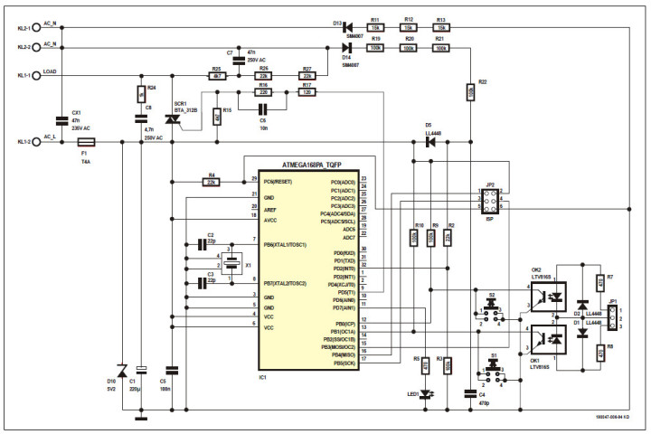
The MCU clock is controlled by crystal X1 to ensure precise timing of the trigger pulses. The network formed by diode D12 and the voltage divider R2, R3 and R19-R22 generates a signal suitable for zero crossing detection, which is clipped to VCC by diode D5.
The gate current is limited by R16 and R17. Fast triggering of the triac is provided by C6 in parallel with R16. A snubber formed by R24 and C8 is connected across T2 and T1 of the triac to prevent false triggering. The triac used here is a Hi-Com type, so the combination of a small capacitance and relatively high resistance is sufficient.
The optional auxiliary load, consisting of R25-R27 and C7, is a special feature. It is only required if the external load has high inductance, such as a transformer. These components are usually not fitted. Capacitor CX1 suppresses RFI.
The module is operated using the pushbutton switches S1 and S2. This can also be done with optocouplers OK1 and OK2 connected in parallel with the switches. Switches with long actuator pins should be used to ensure adequate safety distances. LED1 acts as a power indicator. The microcontroller (IC1) is programmed through the ISP interface on JP2. Fuse F1 at the AC mains input protects the circuit in the event of a short circuit.
Software
The project software was written using the Arduino IDE. It can be downloaded below under ATTACHMENT. However, the author did not use the Arduino functions because they are too slow. The program created by the author is very fast and operates in real time. The sketches were there therefore intentionally not ported to Atmel Studio.
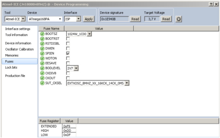
Unfortunately, it is not possible to use the boot loader to program the microcontroller. So much current would be needed at switch-on that the supply voltage would not rise. This means that the fuses must be set to disable the boot loader. The microcontroller can be programmed directly from Atmel Studio using a suitable ISP programmer.
For each app, the project folder contains the corresponding sketch and the hex file. In the initial programming, it is essential to program the fuses as shown in Figure 5.
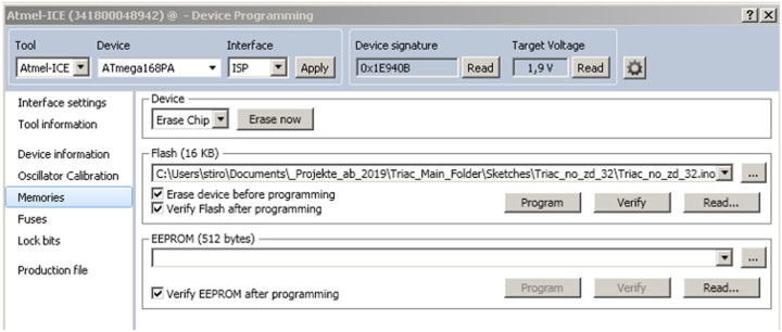
Then the desired hex file can be loaded from the project folder and flashed in the MCU (see Figure 6).
If a sketch is modified, it must be recompiled (verify and compile). The IDE status field shows the folder containing the generated hex file. An example of a typical file path is
C:\Users\name\AppData\Local\Temp\buildxyz.tmp/Triac_...ino.hex
As the folder name and build number are reassigned every day, the file also has to be updated daily in Atmel Studio. If the folder AppData is not visible in File Explorer, select Show hidden files and folders under View/Options.
Then load the desired hex file in Atmel Studio and program the ATmega microcontroller.
Warning: For programming, the module must be fully separated from the AC mains and powered by a safe low-voltage supply.
Applications
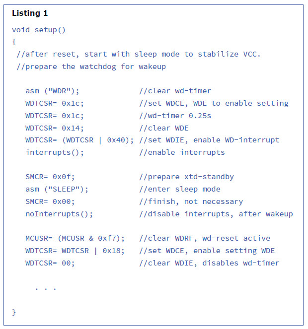
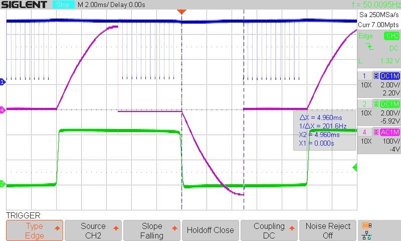
All apps have the same initialisation procedure. On power-up, the BOD level of 2.7 V determines the end of the reset interval. After the following program start, the watchdog timer is activated and the program is put into sleep mode. This allows VCC to rise quickly and reliably (Figure 7). The WD timeout triggers the WD interrupt and terminates sleep mode. Then execution of the actual program starts.
The sketch excerpt in Listing 1 shows how setting the WD timer and sleep mode is implemented. The listing contains part of the code of the initialisation procedure. First the watchdog is set and activated. Then the microcontroller is put into sleep mode. The WD timeout triggers the WD interrupt, which wakes up the microcontroller.
A separate sketch is available for each example app. Each app has its own distinct functions, which can be selected using pushbuttons or jumpers. More information is available in the comments of the individual sketches.
A simple switch and timer app
The Sketch Triac_no_zd_32 app manages without zero crossing detection, so it illustrates the basic programming of the module and its features. The module is operated from a 5 V AC power adapter for programming and testing. If you are interested in hardware-level programming of the WD timer, the various sleep modes, the interrupts, the timer functions or the I/O commands, you should study the code in detail. All of the software can be downloaded free of charge below, under ATTACHMENT.
With this app the module can act as a switch or as a timer, with the actual function selected by a pushbutton. With the additional operating mode ‘Autostart’, the timer starts running immediately after power-up and the load is switched off when the timer period expires. This function can be used to limit how long a lamp remains on. The switch-off time is stored in the program.
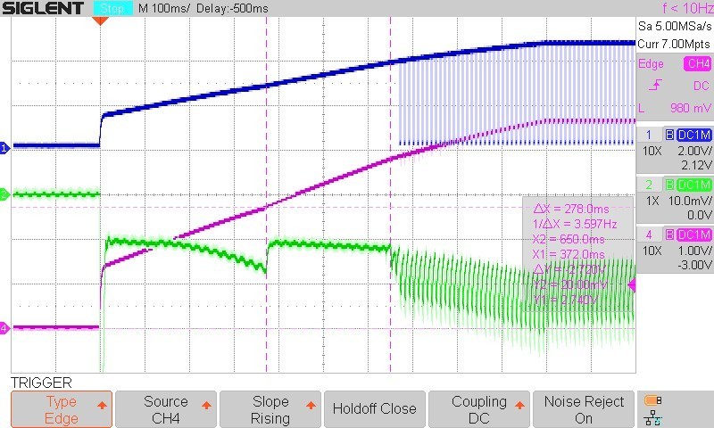
In the on state, the program generates periodic 10 µs pulses with an period of 278 µs to drive the triac. The control pulses are not referenced to the AC mains frequency, so the switching times are not synchronized to the mains voltage. In the worst case, the load will only be switched on 278 µs after the zero crossing. At this point the mains voltage will have already reached 29 V, resulting in voltage spikes that can cause EMC problems. To illustrate this, the oscillogram in Figure 8 shows what happens over an interval of 1 second. The trigger pulses are not correlated to the zero crossings, so they wander with respect to them. The voltage over the triac varies according to the offset between the zero crossing and the trigger pulse.
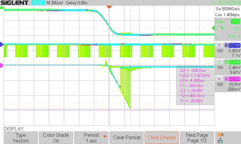
This is remedied in the next practically oriented application, in which the zero crossings are detected so that triac triggering is synchronised with the zero crossings. Unlike the following measurements, the reference voltage here is VCC. T1 of the triac is at VCC, so here you see the control pulses on the gate with negative polarity.
Switch and timer with zero crossing detection
Unlike the previous app, here a signal derived from the AC mains voltage is used to detect the zero crossings of the mains voltage. This signal is applied to the INT0 input, where its falling edges trigger interrupts that mark the start of the first half-wave. The end of this half-wave and the start of the next half-wave are determined by Timer 2. This avoids complicated hardware for precise detection of both zero crossings.
For reliable triggering with low load currents, the first trigger pulse of each half-wave is extended to 280 µs. It is following by two more 10 µs trigger pulses. This ensures that the IL of the triac is exceeded even with high-impedance loads. Figure 9 shows this relationship. The short bumps (approximately 3 V) in the voltage on the triac at the end of each half-wave are particularly noteworthy. They result from the relatively low current through the connected LED lamp, which drops below IH at the end of each half-wave. However, this has little impact on the noise level.
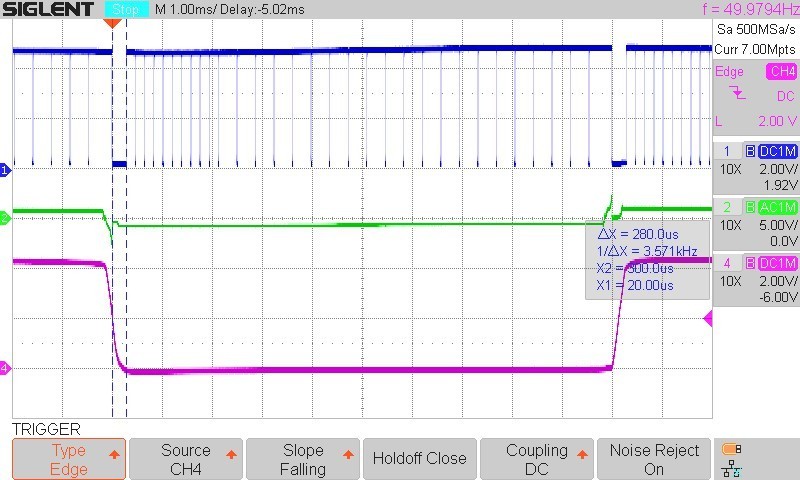
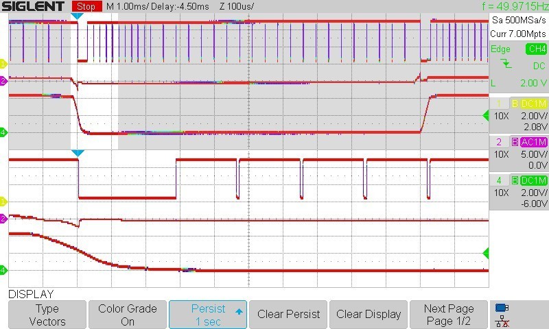
Figure 10 shows the superimposed traces over an interval of 1 second. The control pulses are synchronous with the mains voltage.
Dimmer
Dimming the brightness of a lamp is a typical application for a triac. The lamp power is adjusted by phase angle control. Here the switch-on point of the load (phase angle) is varied with respect to the zero crossing point of each half-wave of the mains voltage. Dimmers can cause a lot of EMC problems because they generate voltage waveforms with high amplitudes and steep edges, depending on the phase angle. The worst case is switching at the crest of the mains voltage (with a phase angle of 90°). When the triac is triggered, the voltage on the triac quickly drops from the crest value to zero (Figure 11). Depending on the load, this results in very high currents and high noise levels. An upstream RFI filter (for example, from a discarded dimmer) is therefore essential.
Many LED lamps do not work with conventional dimmers, due to the design of their power supply. This module also has difficulties with quite a few LED lamps. You should therefore use dimmable lamps.
An interesting feature of this triac control is that after the first pulse, additional pulses are inserted until the end of the half-wave. This allows the module to be used with relatively complex loads. At full power, the first pulse after the zero crossing is extended to 190 µs. This ensures that IH is exceeded even with high-impedance loads.
The output power can be set with the two pushbuttons or with optocouplers.
Soft start for inductive loads
Inductive loads, especially transformers, can draw very high switch-on currents. Here switching at the voltage zero crossing is the most difficult situation. The residual magnetisation of the core can also cause problems, because the switch-on current waveform may be offset from the zero line. As a result, the flux density in the core (the hysteresis loop) is shifted in one direction and can easily enter the saturation region. When that occurs, the winding inductance suddenly drops to zero and the rising current is only limited by the resistance of the winding and other elements. Ring-core transformers are especially prone to this. They should therefore be fused at a significantly higher level than what is required solely for the load current.
Sometimes a varistor or series resistor with a time-delay relay is used to limit the switch-on current until a symmetrical magnetic field (and correspondingly clean AC voltage) is established. In theory, this problem can also be encountered if the phase angle is slowly increased. When switching on the transformer, you should start with a phase angle of around 180° and then slowly reduce it to 0°. This is exactly what is done in this app.
Figure 12 shows the pulse sequence after a restart. The first trigger pulse is generated approximately 8.6 ms after the zero crossing. Another pulse is added ahead of it after each full wave, until the time is reduced to around 0.3 ms.
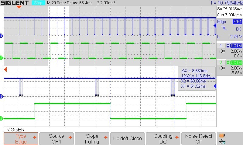
Figure 13 shows the situation after settling down. Within the first 3 ms, the load current goes through zero due to the phase shift. In order to achieve a continuous current flow, it is necessary to put the control pulses close together in this interval.
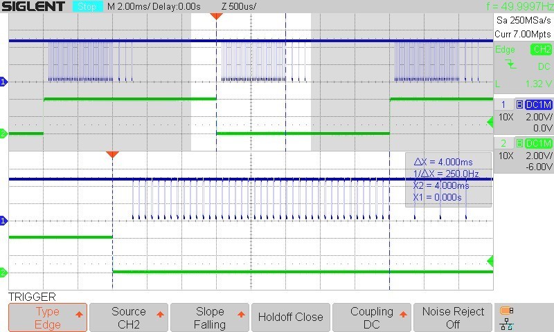
Figure 14 shows the transformer current with no load. The zero crossing signal shows the relationship to the mains voltage. Here you can see the magnetisation current, which reaches a maximum at the voltage zero crossing. The remaining part results from the iron and copper losses of the transformer. The phase lag of the current is not exactly 90°, due to losses and nonlinearities in the core.
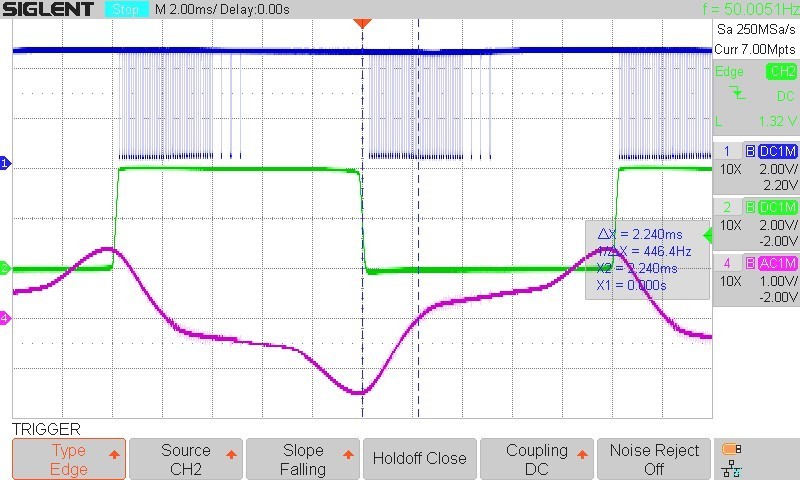
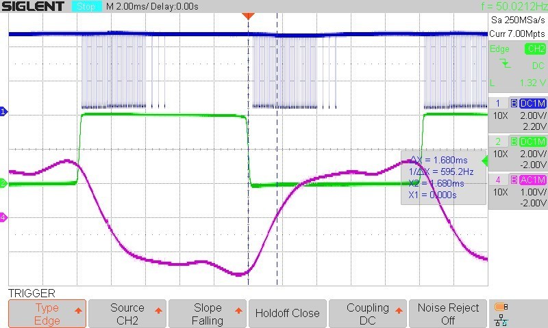
Figure 15 shows the transformer current with a load. The load current and magnetisation current are superimposed. The load reduces the phase shift.
A prerequisite for faultless operation is fully symmetrical control of the triac. The control pulses must have the same offset to the zero crossing for both half-waves, so that the phase angle of the current is symmetrical. IGT and especially IH are significant for this. Reliable triggering is ensured by the RC network, which strengthens the leading edge of the gate current pulse. The transformer current must be greater than IH for the triac to remain conducting. Ring-core transformers are difficult in this regard due to their high inductance. This problem can be solved by a small additional resistive load (R25-R27, optional). Some ring-core transformers even require an additional external load.
Particularly with transformers, driving the triac with pulses alone was a challenge in the programming of the firmware. The various tricks can be easily understood from the detailed comments in the code.
We hope you enjoy the apps described here. Maybe you have an idea for a new application? That’s easy to do by modifying the firmware.
(190047-04)
Want more great Elektor content like this?
Then take out an Elektor membership today and never miss an article, project, or tutorial.
Discussion (0 comments)