
32-bit I2S sine wave generator [200253]
32-bit I2S with ATmega328P, 1 kHz sine wave, fs 192 kHz, level adjustable from 0 to -110 dB in 16 steps
This circuit was designed to test our Audio DAC for the Raspberry Pi (160198), or any DAC with I2S inputs, without having to use a RPi. See https://www.elektormagazine.com/labs/audio-dac-for-rpi-networked-audio-player-using-volumio. If for some reason the analog audio output signal is missing and it’s not clear if the RPi has a problem (software and/or hardware) or the DAC this circuit can provide an answer. Another setup that could work is to use a 24- bit ADC with I2S outputs and an ordinary signal (sine wave) generator as an input source. But, to check if the analog output signals of the DAC are indeed flawless the sine wave of the I2S signal must be perfect to perform proper distortion measurements. The test signal should not be degraded by the analog source and ADC in any way. The use of a micro-controller that supports I2S is an option, but why not use a very common microcontroller like the ATmega328P. Problem is of course, it doesn’t support I2S. It makes it a challenge if it’s possible with the help of additional hardware to make a digital sine wave generator with I2S bus using this microcontroller. This circuit and software show it can be done.
The intent is to create an I2S signal with a sample rate of 192 kHz and 32-bit data. This is close to the maximum sample frequency of the DAC mentioned before. The serial clock (SCK or SCLK) must be 12.288 MHz (2 channels * 192 kHz * 32 bit). The clock of the microcontroller is 20 MHz maximum, although some say it can be clocked with 25 MHz without any problems. The only way to output serial data (SD or SDATA) faster is to use an external parallel-in serial-out shift register and use the clock of the microcontroller to clock the shift register. PB0 must be set as CLKO when programming the fuses. With the aid of the shift register the microcontroller has 8 clock cycles to process each byte. In BASCOM-AVR the following instruction PORTD = A(n), where A(n) is an element of a byte array, only takes 5 clock cycles when used in Do-Loop, surprisingly fast. But if used in a For-To-Next loop each byte lasts several microseconds and is too slow. To make each byte take 8 clock cycles 3 NOPs must be added, after every byte. It takes the Do-Loop 3 clock cycles to restart, which is perfect to produce one full period of 192 samples of a 1 kHz sine wave. So, the main program (Do-Loop) only outputs the bytes of the array to port D. Anything else like calculating the 32-bit sine wave and create the array of byte must be done before the main program starts. The 32-bit samples are divided into four bytes. This means the size of the array must be 4 *192 = 368 bytes. Left and right channel have the same signal and hence each group of 4 bytes per sample must be repeated. The number of lines this part of the main program takes can now be calculated: 2 channels * 4 bytes * 192 samples * 4 lines – 3 = 6141 program lines. The last number 4 consists of 1 statement followed by 3 NOPs. And three lines less because no NOPs are needed when the loop restarts.
A timing diagram can help to choose the external components. The I2S bus has 3 signals. The serial data is clocked on the leading (low-to-high) edge of the serial clock. The word select line (WS or LRCLK) indicates the channel: 0 is left, 1 is right. Its frequency is equal to the sampling frequency of the digital audio signal, here 192 kHz, and can be derived from the serial clock. The serial data and word select line both must change on the trailing (HIGH-to-LOW) edge of the serial clock. The HC-logic family is in principle fast enough to be used for the external components, although propagation delay of the gates must be corrected at one point. 12 ns delay is almost 15 percent of the micro-controller’s clock period. However, as a divider a 74AC4040 (IC3, 12-stage binary ripple counter) must be used to properly align all signals. It’s obsolete but still available at different distributors. The counter advances on the trailing edge of the clock input. It also has a master reset (pin 11) that can be used to synchronize the counter with the micro-controller. The 6th flip-flop (pin 2) divides 12.288 MHz by 64 and outputs exactly 192 kHz, necessary for the word select line. The 6th flip-flop is called either Q5 or Q6, depending on which datasheet you look at. It depends on the manufacturer. Q6 is maybe preferable because this output divides the clock by 2^6. As a shift register 8-bit parallel-in/serial out shift register 74HC165 (IC2) is used. It has an active low parallel load (pin 1) and a clock (pin 2) with inhibit (pin 15, active low enable) which have the same functionality (both internally connected to an OR gate). Depending on component placement swapping connections can simplify routing. Data is shifted on the leading edge of the clock. The serial input (pin 10) is not used and connected to ground. The load pulse (LD, active low) for the shift register is derived from counter output Q4 using Quad 2-Input Exclusive-OR 74HC86 (IC4). The signal to pin 4 is inverted and delayed by IC4A by its propagation delay and an extra delay of a few nanoseconds by R4/C4. Because of the Exclusive-OR function each change of Q4 gives a short active low pulse at the output of IC4B. The pulse is long enough to load the new data into the shift register but short enough to be inactive before the leading edge of the clock. To load the data from port D into the shift register at the correct moment the pulse must be active just after the leading edge of the clock (pin 1). This means the clock of the shift register must be inverted, done by IC4C. The most significant bit of the serial data of the I2S bus is located one clock period after the change of word select. An extra D-type flip-flop is needed. Selected is a 74HC74 (IC5), a dual D-type flip-flop with set and reset and positive edge-trigger. By doing so, the signal for SDATA is delayed. To compensate for this the inverted clock signal of IC4C is inverted again by IC4D to make the serial clock line up with the serial data.
Software:
The purpose of the circuit is to create a perfect 1 kHz sine wave with 32-bit accuracy. First BASCOM-AVRs own instruction for trigonometric function SIN(x) was used but wasn’t accurate enough, as following example shows:
DIM Pi,A,X As Single
Pi = 3.1415926535897932384626433
X = Pi / 2
A = SIN(X)
Print "Sin(Pi/2) = " ; A
End
This piece of code results in: Sin(Pi/2) = 0.99999332
But variable A should be exactly 1. For X = Pi/6 the result is 0.499993796, but should be exactly 0.5. So, for calculating an extreme accurate sine wave this is not accurate enough. The only option is to calculate the sine wave by using the Taylor polynomial for SIN(X) with enough terms:
SIN(X) = X-(X^3)/3!+(X^5)/5!-(X^7)/7!+(X^9)/9!-(X^11)/11!+(X^13)/13!-(X^15)/15!
In BASCOM-AVR a calculation can only be performed on two operands. The polynomial is calculated in many segments:
Xn = X * X
Xn = Xn * X 'Xn = X^3
DIV = Xn/F3
SINX = X - DIV
Xn = Xn * X
Xn = Xn * X 'Xn = X^5
DIV = Xn/F5
SINX = SINX + DIV
Xn = Xn * X
Xn = Xn * X 'Xn = X^7
DIV = Xn/F7
SINX = SINX - DIV
Xn = Xn * X
Xn = Xn * X 'Xn = X^9
DIV = Xn/F9
SINX = SINX + DIV
Xn = Xn * X
Xn = Xn * X 'Xn = X^11
DIV = Xn/F11
SINX = SINX - DIV
Xn = Xn * X
Xn = Xn * X 'Xn = X^13
DIV = Xn/F13
SINX = SINX + DIV
Xn = Xn * X
Xn = Xn * X 'Xn = X^15
DIV = Xn/F15
SINX = SINX - DIV
To speed things up the factorial calculations are avoided and variables with the correct value are used instead (F3 = 6 … F15 = 1307674368000). All variables in calculations are of type Double, signed 64 bit binary numbers (8 bytes, 5 x 10^-324 to 3.4 x 10^308). Using the Taylor polynomial:
Sin(Pi/6) = 500E-3
Sin(Pi/2) = 999.999999993977E-3
To divide the result of the calculation of SIN(X) into 4 bytes it must first be converted to a variable of type Long, signed 32-bit binary numbers (-2147483648 to 2147483647). The result of the calculation is maximal 1 or -1. If we want the 32-bit data to have a full-scale level the value of SIN(X) must multiplied by (2^32)/2 - 1:
SINX = SINX * U
Where U = 2147483647
The conversion to Long can be done in just one statement, a Long variable gets the value of a Double variable. Now, the result of the calculation is available as signed 32-bit:
SINXlong = SINX
Dividing into 4 bytes is just a matter of shifting the bits of SINXlong and store them in 4 variables of type Byte. A subroutine called SampleX does all these calculations for any value of X. But, the calculation proved to be only truly accurate for X = -π/2 through +π/2. So, first the sine wave is calculated from -π/2 through +π/2, taking 97 samples (4 bytes per sample). The rest of the array is complemented by mirroring the elements of the first array per group of 4 bytes, taking 95 samples. Sample 193 is the same as the first of the array (4 bytes). The Do-Loop restarts.
Instead of just producing a 1 kHz sine wave at a fixed level, 4 inputs of port C (pull-ups) are connected to a hexadecimal coded rotary (SD-1010) to set the output level. There are ‘real code’ and ‘complementary code’ type of rotary coded switches. The first type is used here. All switches are open for 0. Whatever type is used the software must be written accordingly. A 4-way DIP-switch could have been used instead but changing levels is easier with the rotary switch, much like an analog volume control. This feature can be used to check linearity of the DAC. For a different level the microcontroller must be reset each time, hence the presence of reset button S2. For each different level-setting a Select Case statement is used to set the correction-factor U (type Double) to the correct value:
Select Case S1
Case 15 : 'S1 = 0
U = 2147483647 '0 dB
Case 14 : 'S1 = 1
U = 1913946815 '-1 dB
Case 13 : 'S1 = 2
U = 1705806894 '-2 dB
Case 12 : 'S1 = 3
U = 1520301995 '-3 dB
Case 11 : 'S1 = 4
U = 1076291388 '-6 dB
Case 10 : 'S1 = 5
U = 679093956.2 '-10 dB
Case 9 : 'S1 = 6
U = 214748365.7 '-20 dB
Case 8 : 'S1 = 7
U = 67909395.62 '-30 dB
Case 7 : 'S1 = 8
U = 21474836.47 '- 40 dB
Case 6 : 'S1 = 9
U = 6790939.562 '-50 dB
Case 5 : 'S1 = A
U = 2147483.647 '-60 dB
Case 4 : 'S1 = B
U = 679093.9562 '-70 dB
Case 3 : 'S1 = C
U = 214748.3647 '-80 dB
Case 2 : 'S1 = D
U = 67909.39562 '-90 dB
Case 1 : 'S1 = E
U = 21474.83647 '-100 dB
Case 0 : ‘S1 = F
U = 6790.939562 '-110 dB
End Select
The correct values for each output level are entered in the program to avoid extra calculations but also because calculating these factors in the program wasn’t accurate enough. Selecting this correction-factor must be done before the samples of the sine wave are calculated, it’s used for all samples.
At the beginning of the program the reset of the counter (IC3) is activated (high). Just before the start of the main program it’s deactivated, about a quarter of a second after power up. That’s all the time it takes to create the array. This synchronizes the data at the output of the shift register and the word select line. First 3 samples, with value 0, and a few NOPs are used so the first byte is at the output of SDATA at the correct moment. There is a window of 7 clock cycles for the first MS-byte to be clocked into the shift register. Each byte at port D is replaced by the next after 8 clock cycles. In other words, the moment the first MS-byte at port D can change relative to the load pulse of the shift register may vary 7 clock cycles (see timing diagram). The data at the output of port D changes a few nanoseconds after the leading edge of CLKO (PB0).
It is possible to create an array with only samples of the sine wave from -π/2 through +π/2 and select the correct array elements in the main program to complete the data for a full sine wave period at port D. But, instead of a sine wave a more complex signal that isn’t as symmetrical can be interesting for other purposes. And if a complete array is used in the main program it’s easier to read. There are still a few IO’s of the microcontroller unused and can be used to change the waveform or frequency by augmenting the software. Food for thought…PB2, PC0 and PC1 can be used without any problem. PB4 and PB5 are used for In System Programming (ISP) and care must be taken additional connected components don’t interfere with the ISP. LED1 was added to show the processor is calculating first, but since this is done in only a quarter of second PB3 can also be used for additional features. In that case R1 could be connected to the power supply to indicate power-on. The program uses 77 % of the flash memory. Just calculating the sine wave as described about 10 %. So, extending the code and adding extra features is possible.
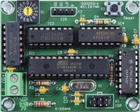
The PCB is according to the schematic. Should a 74AC4040 no longer be available, it is possible to cut the track between the pads of pin 13 and 14 of IC4. By connecting pin13 to ground by a piece of wire a HC version can be used, but timing is far from optimal and could pose a problem with the DAC being tested. This correction works with our RPi DAC. The wires between the DAC and the generator should be kept as short as possible.
Measurements
Power supply current is 21 mA at 3.3 V.
THD+N of the latest batch of our RPi Audio DAC 0.0013 % (1.088 V/load 10 kΩ, B = 22 kHz)
It uses an OPA1611A in the output stage (originally LME49710MA)
Bill of materials (all parts are through hole)
Resistors
R1 = 2.2 kΩ
R2 = 100 Ω
R3 = 10 kΩ
R4 = 150 Ω
Capacitor
C1,C2,C4 = 22 pF, lead spacing 5 mm
C3,C5,C6,C7,C8,C9 = 100 nF, ceramic, lead spacing 5 mm
Semiconductor
LED1 = green 3 mm led
IC1 = ATmega328P-20PU, DIP-28
IC2 = 74HC165, DIP-16
IC3 = 74AC4040, DIP-16 (don’t use HC, see text)
IC4 = 74HC86, DIP-14
IC5 = 74HC74, DIP-14
Other
K1 = 2x3 pin header, vertical, pitch 2.54 mm
K2 = 1x4 pin header, vertical, pitch 2.54 mm
K3 = 2way screw terminal, pitch 5 mm
S1 = hexadecimal coded rotary switch SD-1010 (Nidec Copal Electronics)
S2 = 6 mm tactile switch, SPST-NO
X1 = 12.288 MHz crystal, HC-49
The intent is to create an I2S signal with a sample rate of 192 kHz and 32-bit data. This is close to the maximum sample frequency of the DAC mentioned before. The serial clock (SCK or SCLK) must be 12.288 MHz (2 channels * 192 kHz * 32 bit). The clock of the microcontroller is 20 MHz maximum, although some say it can be clocked with 25 MHz without any problems. The only way to output serial data (SD or SDATA) faster is to use an external parallel-in serial-out shift register and use the clock of the microcontroller to clock the shift register. PB0 must be set as CLKO when programming the fuses. With the aid of the shift register the microcontroller has 8 clock cycles to process each byte. In BASCOM-AVR the following instruction PORTD = A(n), where A(n) is an element of a byte array, only takes 5 clock cycles when used in Do-Loop, surprisingly fast. But if used in a For-To-Next loop each byte lasts several microseconds and is too slow. To make each byte take 8 clock cycles 3 NOPs must be added, after every byte. It takes the Do-Loop 3 clock cycles to restart, which is perfect to produce one full period of 192 samples of a 1 kHz sine wave. So, the main program (Do-Loop) only outputs the bytes of the array to port D. Anything else like calculating the 32-bit sine wave and create the array of byte must be done before the main program starts. The 32-bit samples are divided into four bytes. This means the size of the array must be 4 *192 = 368 bytes. Left and right channel have the same signal and hence each group of 4 bytes per sample must be repeated. The number of lines this part of the main program takes can now be calculated: 2 channels * 4 bytes * 192 samples * 4 lines – 3 = 6141 program lines. The last number 4 consists of 1 statement followed by 3 NOPs. And three lines less because no NOPs are needed when the loop restarts.
A timing diagram can help to choose the external components. The I2S bus has 3 signals. The serial data is clocked on the leading (low-to-high) edge of the serial clock. The word select line (WS or LRCLK) indicates the channel: 0 is left, 1 is right. Its frequency is equal to the sampling frequency of the digital audio signal, here 192 kHz, and can be derived from the serial clock. The serial data and word select line both must change on the trailing (HIGH-to-LOW) edge of the serial clock. The HC-logic family is in principle fast enough to be used for the external components, although propagation delay of the gates must be corrected at one point. 12 ns delay is almost 15 percent of the micro-controller’s clock period. However, as a divider a 74AC4040 (IC3, 12-stage binary ripple counter) must be used to properly align all signals. It’s obsolete but still available at different distributors. The counter advances on the trailing edge of the clock input. It also has a master reset (pin 11) that can be used to synchronize the counter with the micro-controller. The 6th flip-flop (pin 2) divides 12.288 MHz by 64 and outputs exactly 192 kHz, necessary for the word select line. The 6th flip-flop is called either Q5 or Q6, depending on which datasheet you look at. It depends on the manufacturer. Q6 is maybe preferable because this output divides the clock by 2^6. As a shift register 8-bit parallel-in/serial out shift register 74HC165 (IC2) is used. It has an active low parallel load (pin 1) and a clock (pin 2) with inhibit (pin 15, active low enable) which have the same functionality (both internally connected to an OR gate). Depending on component placement swapping connections can simplify routing. Data is shifted on the leading edge of the clock. The serial input (pin 10) is not used and connected to ground. The load pulse (LD, active low) for the shift register is derived from counter output Q4 using Quad 2-Input Exclusive-OR 74HC86 (IC4). The signal to pin 4 is inverted and delayed by IC4A by its propagation delay and an extra delay of a few nanoseconds by R4/C4. Because of the Exclusive-OR function each change of Q4 gives a short active low pulse at the output of IC4B. The pulse is long enough to load the new data into the shift register but short enough to be inactive before the leading edge of the clock. To load the data from port D into the shift register at the correct moment the pulse must be active just after the leading edge of the clock (pin 1). This means the clock of the shift register must be inverted, done by IC4C. The most significant bit of the serial data of the I2S bus is located one clock period after the change of word select. An extra D-type flip-flop is needed. Selected is a 74HC74 (IC5), a dual D-type flip-flop with set and reset and positive edge-trigger. By doing so, the signal for SDATA is delayed. To compensate for this the inverted clock signal of IC4C is inverted again by IC4D to make the serial clock line up with the serial data.
Software:
The purpose of the circuit is to create a perfect 1 kHz sine wave with 32-bit accuracy. First BASCOM-AVRs own instruction for trigonometric function SIN(x) was used but wasn’t accurate enough, as following example shows:
DIM Pi,A,X As Single
Pi = 3.1415926535897932384626433
X = Pi / 2
A = SIN(X)
Print "Sin(Pi/2) = " ; A
End
This piece of code results in: Sin(Pi/2) = 0.99999332
But variable A should be exactly 1. For X = Pi/6 the result is 0.499993796, but should be exactly 0.5. So, for calculating an extreme accurate sine wave this is not accurate enough. The only option is to calculate the sine wave by using the Taylor polynomial for SIN(X) with enough terms:
SIN(X) = X-(X^3)/3!+(X^5)/5!-(X^7)/7!+(X^9)/9!-(X^11)/11!+(X^13)/13!-(X^15)/15!
In BASCOM-AVR a calculation can only be performed on two operands. The polynomial is calculated in many segments:
Xn = X * X
Xn = Xn * X 'Xn = X^3
DIV = Xn/F3
SINX = X - DIV
Xn = Xn * X
Xn = Xn * X 'Xn = X^5
DIV = Xn/F5
SINX = SINX + DIV
Xn = Xn * X
Xn = Xn * X 'Xn = X^7
DIV = Xn/F7
SINX = SINX - DIV
Xn = Xn * X
Xn = Xn * X 'Xn = X^9
DIV = Xn/F9
SINX = SINX + DIV
Xn = Xn * X
Xn = Xn * X 'Xn = X^11
DIV = Xn/F11
SINX = SINX - DIV
Xn = Xn * X
Xn = Xn * X 'Xn = X^13
DIV = Xn/F13
SINX = SINX + DIV
Xn = Xn * X
Xn = Xn * X 'Xn = X^15
DIV = Xn/F15
SINX = SINX - DIV
To speed things up the factorial calculations are avoided and variables with the correct value are used instead (F3 = 6 … F15 = 1307674368000). All variables in calculations are of type Double, signed 64 bit binary numbers (8 bytes, 5 x 10^-324 to 3.4 x 10^308). Using the Taylor polynomial:
Sin(Pi/6) = 500E-3
Sin(Pi/2) = 999.999999993977E-3
To divide the result of the calculation of SIN(X) into 4 bytes it must first be converted to a variable of type Long, signed 32-bit binary numbers (-2147483648 to 2147483647). The result of the calculation is maximal 1 or -1. If we want the 32-bit data to have a full-scale level the value of SIN(X) must multiplied by (2^32)/2 - 1:
SINX = SINX * U
Where U = 2147483647
The conversion to Long can be done in just one statement, a Long variable gets the value of a Double variable. Now, the result of the calculation is available as signed 32-bit:
SINXlong = SINX
Dividing into 4 bytes is just a matter of shifting the bits of SINXlong and store them in 4 variables of type Byte. A subroutine called SampleX does all these calculations for any value of X. But, the calculation proved to be only truly accurate for X = -π/2 through +π/2. So, first the sine wave is calculated from -π/2 through +π/2, taking 97 samples (4 bytes per sample). The rest of the array is complemented by mirroring the elements of the first array per group of 4 bytes, taking 95 samples. Sample 193 is the same as the first of the array (4 bytes). The Do-Loop restarts.
Instead of just producing a 1 kHz sine wave at a fixed level, 4 inputs of port C (pull-ups) are connected to a hexadecimal coded rotary (SD-1010) to set the output level. There are ‘real code’ and ‘complementary code’ type of rotary coded switches. The first type is used here. All switches are open for 0. Whatever type is used the software must be written accordingly. A 4-way DIP-switch could have been used instead but changing levels is easier with the rotary switch, much like an analog volume control. This feature can be used to check linearity of the DAC. For a different level the microcontroller must be reset each time, hence the presence of reset button S2. For each different level-setting a Select Case statement is used to set the correction-factor U (type Double) to the correct value:
Select Case S1
Case 15 : 'S1 = 0
U = 2147483647 '0 dB
Case 14 : 'S1 = 1
U = 1913946815 '-1 dB
Case 13 : 'S1 = 2
U = 1705806894 '-2 dB
Case 12 : 'S1 = 3
U = 1520301995 '-3 dB
Case 11 : 'S1 = 4
U = 1076291388 '-6 dB
Case 10 : 'S1 = 5
U = 679093956.2 '-10 dB
Case 9 : 'S1 = 6
U = 214748365.7 '-20 dB
Case 8 : 'S1 = 7
U = 67909395.62 '-30 dB
Case 7 : 'S1 = 8
U = 21474836.47 '- 40 dB
Case 6 : 'S1 = 9
U = 6790939.562 '-50 dB
Case 5 : 'S1 = A
U = 2147483.647 '-60 dB
Case 4 : 'S1 = B
U = 679093.9562 '-70 dB
Case 3 : 'S1 = C
U = 214748.3647 '-80 dB
Case 2 : 'S1 = D
U = 67909.39562 '-90 dB
Case 1 : 'S1 = E
U = 21474.83647 '-100 dB
Case 0 : ‘S1 = F
U = 6790.939562 '-110 dB
End Select
The correct values for each output level are entered in the program to avoid extra calculations but also because calculating these factors in the program wasn’t accurate enough. Selecting this correction-factor must be done before the samples of the sine wave are calculated, it’s used for all samples.
At the beginning of the program the reset of the counter (IC3) is activated (high). Just before the start of the main program it’s deactivated, about a quarter of a second after power up. That’s all the time it takes to create the array. This synchronizes the data at the output of the shift register and the word select line. First 3 samples, with value 0, and a few NOPs are used so the first byte is at the output of SDATA at the correct moment. There is a window of 7 clock cycles for the first MS-byte to be clocked into the shift register. Each byte at port D is replaced by the next after 8 clock cycles. In other words, the moment the first MS-byte at port D can change relative to the load pulse of the shift register may vary 7 clock cycles (see timing diagram). The data at the output of port D changes a few nanoseconds after the leading edge of CLKO (PB0).
It is possible to create an array with only samples of the sine wave from -π/2 through +π/2 and select the correct array elements in the main program to complete the data for a full sine wave period at port D. But, instead of a sine wave a more complex signal that isn’t as symmetrical can be interesting for other purposes. And if a complete array is used in the main program it’s easier to read. There are still a few IO’s of the microcontroller unused and can be used to change the waveform or frequency by augmenting the software. Food for thought…PB2, PC0 and PC1 can be used without any problem. PB4 and PB5 are used for In System Programming (ISP) and care must be taken additional connected components don’t interfere with the ISP. LED1 was added to show the processor is calculating first, but since this is done in only a quarter of second PB3 can also be used for additional features. In that case R1 could be connected to the power supply to indicate power-on. The program uses 77 % of the flash memory. Just calculating the sine wave as described about 10 %. So, extending the code and adding extra features is possible.
The PCB is according to the schematic. Should a 74AC4040 no longer be available, it is possible to cut the track between the pads of pin 13 and 14 of IC4. By connecting pin13 to ground by a piece of wire a HC version can be used, but timing is far from optimal and could pose a problem with the DAC being tested. This correction works with our RPi DAC. The wires between the DAC and the generator should be kept as short as possible.
Measurements
Power supply current is 21 mA at 3.3 V.
THD+N of the latest batch of our RPi Audio DAC 0.0013 % (1.088 V/load 10 kΩ, B = 22 kHz)
It uses an OPA1611A in the output stage (originally LME49710MA)
Bill of materials (all parts are through hole)
Resistors
R1 = 2.2 kΩ
R2 = 100 Ω
R3 = 10 kΩ
R4 = 150 Ω
Capacitor
C1,C2,C4 = 22 pF, lead spacing 5 mm
C3,C5,C6,C7,C8,C9 = 100 nF, ceramic, lead spacing 5 mm
Semiconductor
LED1 = green 3 mm led
IC1 = ATmega328P-20PU, DIP-28
IC2 = 74HC165, DIP-16
IC3 = 74AC4040, DIP-16 (don’t use HC, see text)
IC4 = 74HC86, DIP-14
IC5 = 74HC74, DIP-14
Other
K1 = 2x3 pin header, vertical, pitch 2.54 mm
K2 = 1x4 pin header, vertical, pitch 2.54 mm
K3 = 2way screw terminal, pitch 5 mm
S1 = hexadecimal coded rotary switch SD-1010 (Nidec Copal Electronics)
S2 = 6 mm tactile switch, SPST-NO
X1 = 12.288 MHz crystal, HC-49
Discussion (3 comments)