
6-Channel Temperature Monitor & Logger [130548]
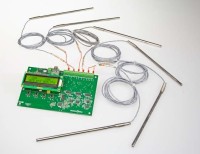
Six-channel temperature monitor, scanner cq data logger for RTD resistive Pt100 sensors.
Because we like to measure temperature so much, we decided to design a device capable of measuring up to six of them. Usually, thermometers only measure one temperature — some can do two, often labelled ‘inside’ and ‘outside’ — but for process control more channels may be required. Range is also important, which is why the device presented here can measure temperatures from as low as −240 °C up to +850 °C. Note that these are software limits; the real-world limits greatly depend on the sensors being used.
Resistance thermometers
To measure temperature, we will use so-called RTDs in the shape of Pt100 probes. RTD is short for Resistance Temperature Detector, a device consisting of a length of metal wire with a known resistance/temperature relationship spiralled on some supporting material. The metal used typically is platinum, copper or nickel. Sensor precision depends on the purity of the metal. Platinum has the most stable resistance/temperature relationship over the largest temperature range.
A Pt100 probe is an RTD made from platinum wire (‘Pt’ in the Periodic Table). The value ‘100’ indicates that its resistance is 100 Ω at 0 °C. Other values can be had too, like 500, 1000 or even 2000. Pt100 sensors are widely used and easy to find. They come in different quality grades — classes — that determine their price, range, accuracy and precision. They also come with a variable number of connecting wires: 2, 3 or 4. The extra wires are used to measure the resistance of the RTD’s connecting wires (more on that later). As these wires — that can be rather long — behave themselves as imprecise RTDs, it is important to compensate the sensor for them to ensure accurate results. To avoid complicating our system too much, we opted for 3-wire RTDs.
An RTD is not a thermocouple
This is important to understand. A thermocouple is a junction of two different metals that produces a temperature-dependent voltage as a result of the thermoelectric (Seebeck) effect. Therefore, a thermocouple does not need a power source to operate whereas an RTD requires some form of excitation. Thermocouples tend to be less precise than RTDs, but they are very cheap.
Linearity
One last but important thing to mention about RTDs is their slightly curved resistance/temperature relationship. This implies that some calculations must be done to obtain the correct temperature from the measured resistance. The Callendar–Van Dusen equation has long been used for platinum RTDs, but in 1990 the Comité International des Poids et Mesures replaced it by a 12th-order polynomial valid over the temperature range from -259.35 °C to 0 °C and a second, 9th-order polynomial for temperatures from 0 °C up to 961.78 °C. Because evaluating such polynomials necessitates significant computing power (and debugging), most applications simply use lookup tables. We did so too.
Howland current source
As briefly mentioned above, an RTD must be excited in some way to make it usable. Both a constant voltage or constant current source can be used for this. We preferred a constant current source since this poses fewer problems with long sensor wires. In this case the voltage over the sensor only depends on the current and, of course, the temperature, and not also on the resistance of the connecting wires.
Constant current source designs are plentiful but a popular one for use with RTDs is the Howland current source or current pump. This kind of source has the advantage of having a very high output impedance compared to other current source designs and it can sink as well as source current. However, to make it work as intended, the resistors R1 to R4 surrounding the opamp should have a tolerance of better than 1%.
When the ratio R1/R2 is equal to the ratio R3/R4, then the output current is given by:
IRTD = (V+−V−)/R3
Compensating for connecting wires
The figure below also shows how the RTD is connected to the current source with its three wires. If we assume that the three wires are identical and that we can measure the voltages ‘V’ and ‘VRW’ with a very high input impedance (meaning that there is no current flowing in the directions of V and VRW), then the voltage over the RTD is given as:
VRTD = V−2×VRW
This completes our theoretical introduction, and we can move on to studying the actual schematic.
The input multiplexer
Looking at the left of the schematic, we find connectors K3 to K7 for the six RTD channels. One wire of each RTD is connected to GND, the two others to a 4051 multiplexer. IC7 forwards the signal ‘V’ to the rest of the system; IC5 does the same for signal ‘VRW’. The third multiplexer, IC9, works the other way around and connects the output of the current source — constructed around IC10 — to the selected RTD.
Each multiplexer has eight channels, two of which are used for reference signals Vmin (GND) and Vmax (VR3). (Now you finally understand why there are six RTD channels and not seven or five.) These reference signals follow the same paths as the RTD signals (R3, a 0.01% tolerance resistor, is even mounted close to the RTD connectors to make it as similar as an RTD as practically possible). Because the values of these signals are known, this allows the software to calibrate the digitizer stage and remove errors introduced by the multiplexer and current source.
The outputs of the input multiplexer are each amplified by 13 by IC6 and IC8. The signal ‘V’ then ends up at the microcontroller’s ADC input 3 (AIN0.3), whereas signal ‘VRW’ connects to AIN0.5.
Current source, part two
The Howland current source is realized with IC10, and resistors R1, R20, R21 and R22. V+ from our description above is connected to GND and therefore has a value of 0 V. V− is equal to −2.5 V, produced by voltage reference IC11. R21 corresponds to R3 from the description above. The output current therefore is (0 − −2.5)/10,000 = +250 µA.
Power supply
Theoretically, the supply voltage for the circuit connected to K1 can be up to 15 VDC, but this will put unnecessary strain on the low-drop voltage regulators. The minimum supply voltage is 7.5 VDC, the recommended value is 9 VDC. The total current consumption is around 70 mA including the 20 mA consumed by the backlight of LCD1. (Note that the latter has a built-in current limiting resistor.) IC1 lowers the supply voltage to 5◦V for most of the circuit except microcontroller IC4; IC2 creates a 3.3-volt supply for this clever part.
The analogue input stage also requires a −5 V supply voltage, and this is taken care of by IC3.
The microcontroller
Over the past years, we have seen so many Arduino-based circuits passing by that one may have come to believe that there exists only one type of 8-bit microcontroller. That this is not true is proven by our circuit with its pimped-up, 8051-based brain. Now, before turning away in disgust, know that almost forty years after its introduction the 8051 still is a widely used 8-bit processor. Manufactured by Silicon Labs, the C8051F350 MCU used here runs internally at 49 MHz and executes most of its instructions in one cycle, making it a pretty fast device.
The C8051F350 is part of a family of four that differ only in package type and ADC resolution. The ‘F350 is the largest part with a 24-bit sigma-delta ADC, eight dedicated analogue inputs, and 17 digital I/O pins. It is an analogue-oriented controller with built-in digital filters and two 8-bit DACs. In this design we do not use all its capabilities, but you may want to study it further for some future project.
Although running from 3.3 volts, its digital I/O pins are 5◦V tolerant, which is why it interfaces nicely with the 5-volt-powered peripheral circuitry (note the pull-up resistors R4 to R8 and network RN1).
A quartz crystal or resonator is not necessary as the MCU has a calibrated oscillator inside.
Four pushbuttons (S1 to S4) and an LCD provide the user interface. P1 sets the contrast level of the display; if you forget to adjust it when you power the board for the first time, the display will probably not show anything.
For communication with a computer, we added the option to plug a USB-to-TTL-serial converter on the board. We used our own breakout board, but it is also possible to connect some other interface. Please note that the photographs in this article show a prototype which used our (old) FT232R BoB 110553. Since then it has been replaced by our new FT231X BoB 180537 which is compatible with the de facto standard of 'FTDI' USB-to-serial cables.
Let's dive into the software
At the time of writing the kind people of Silicon Labs still handed out free licenses for Keil µVision5 so people who develop software for the C8051 devices in C can do this in a comfortable way. When you request such a license it seems to be valid for just one month, but once installed in the IDE it becomes a permanent license. Of course, we have explored this avenue, and everything went fine, yet you never know when they decide to stop doing this and so we ported our software to SDCC, the open source compiler for 8051 and PIC devices.
SDCC does not work with projects and does not use make nor any other GCC-based tool. Our project therefore is just a bunch of files in a folder together with a batch file to compile them.
As with every C program, the visible part starts in the function main. The first thing to do here is to switch off the watchdog timer; you can always switch it back on later when you are ready for it. (Note that the Keil compiler does this in the runtime (CRT) startup file so you don’t notice it. We found that out the hard way.)
After initializing the MCU’s peripherals — 1 ms system tick timer, UART running at 9600 baud, etc. — the program performs a calibration of the ADC. This is a pretty neat feature of the MCU as it allows us to calibrate away many of the imperfections of our analogue front end. After calibration, converting Vmax — the voltage over 0.01% resistor R3 — will read as 0xffffff (24-bit maximum value) while Vmin (GND) will produce a reading of 0. The ADC applies the corrections in hardware; nothing to do for us in software.
A word on sampling
The rest of the time the main will spin in an endless loop, looking for potential key presses and updating the display when needed. Every second a sample is taken from a channel, converted to a value in degrees Celsius or Fahrenheit and printed to the screen. A second later the next channel in line is updated. In the background the ADC runs at a faster rate of nearly 18.7 Hz. This higher speed is necessary for two reasons. First, to measure one RTD two voltages (‘V’ and ‘VRW’) have to be converted as the RTD value must be compensated for the voltage over the connecting wires. Second, the ADC has a built-in low-pass filter that needs three samples to calculate an output value. Therefore, at least six samples are required for one RTD measurement, which corresponds to 320 ms. By reducing the display time to 1 Hz, the system has enough slack to sample and filter comfortably.
Lookup table
Samples must be converted to temperature values and this is done with the help of a lookup table. Pt100 conversion tables can be found on the Internet and we compiled one from −240 °C to +850 °C with a 10-degree step size. Below −240 °C things become highly inaccurate and so we limited the display to −260 °C (which actually means underflow). For similar reasons the upper limit was fixed at +850 °C.
Of course, most ADC readings will be in between two table values and so linear interpolation is used to estimate the temperature. If more precise conversions are desired, it is possible to make the lookup table’s step size smaller, as long as it fits in memory (of which there is not a lot). If the table becomes large, you might want to implement a more efficient search algorithm than the linear search we used or use a polynomial approximation.
Construction
Even though the project uses mostly SMT parts, assembling the PCB should not be too difficult. Start by mounting 2-terminal parts like resistors and ceramic capacitors and then continue with increasingly taller parts. Respect the polarity of polarized parts like diodes and electrolytic capacitors.
It is always a good idea to build and test the power supply (D2, IC1 and IC2 and the capacitors around them) before mounting the other parts.
Make sure to use resistors with 1% tolerance in the input stage except for R3 which must have a tolerance of 0.01%. To create a real good current source, you might want to use 0.1% tolerance resistors for R1, R20, R21 & R22.
Depending on if and how you mount the USB-serial interface, you may want to use extra-tall connectors for the display as it is mounted over the serial BoB.
Loading the firmware
Connector K2 is used for programming the firmware into the MCU. This connector follows the official Silicon Labs 2-wire C2 programming/debugging interface standard so connecting a C2-compatible programmer should be easy. Less easy, on the other hand, is obtaining such a programmer, which is why we rolled our own. The download accompanying this article includes an Arduino sketch that transforms any Arduino-Uno-compatible board into a C2 programmer. The MCU’s 5◦V-tolerant pins allow us to do this. Connect Arduino pin A0 to K2 pin 7 (‘C2CK’), Arduino pin A1 to K2 pin 4 (‘C2D’), and Arduino GND to K2 pin 2. Connect the Arduino to the computer before powering the board and all should be fine.
A Python 3 script, also included in the download, permits uploading Intel HEX files to the home-brewed programmer. This script requires pySerial.
Using the system
There are two firmwares for this project, one with debugging options (‘d’ suffix) and one without. The main UI functions are the same for both:
- ‘Menu’ (S1): press this button to enter the settings “page”. On this page you can toggle the temperature units between Celsius and Fahrenheit by pressing S1 again. With the keys ‘Decr’ (S2) and ‘Incr’ (S3) you can adjust the display refresh value from one second to one minute. When done, you can either press ‘Save’ (S4) to store the new settings in non-volatile memory or let the page timeout. When the page times out the new settings will be used until the next change or a power cycle.
- ‘Save’ (S4): press to recalibrate the system.
The debug firmware adds to this:
- ‘Decr’ (S2): pressing this key during startup and keeping it pressed until the splash screens have passed will skip ADC calibration at startup. Use ‘Save’ (S4) to calibrate when you want to.
- ‘Decr’ (S2) + ‘Incr’ (S3): pressing these keys at the same time will open the debug page where you can see raw 16-bit ADC values for both the signals ‘V’ (RTD) and ‘VRW’ (Wire). Pressing ‘Incr’ will select the next channel. Press ‘Save’ (S4) to return to normal mode.
Data logging
Plug BOB1 on the board (or use another USB-to-serial converter, the connections are compatible with an 'FTDI' cable) and connect it to a free USB port on a PC. The latter should detect it as a serial port. Launch a terminal program and configure it for 9600 baud, eight data bits, no parity and one stop bit (9600n81). As soon as the board is powered, it will start sending comma-separated values (CSV) in human-readable ASCII format. Most serial port terminal programs will allow you to record the data to a file so it can be processed further in for instance a spreadsheet.
Discussion (3 comments)