
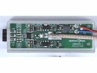
Differential Current Probe [180665]
Differential current probe with single-ended output, +/-18 V supply voltage, 6 MHz bandwidth, and gain of 2, set by a single resistor, can be increased.
Designed by A. Rosenkränzer
This current probe has a differential input and single ended output. Instrumentation amplifier AD8421 is used for its high bandwidth. The amplifier is configured for a gain of 2, set by a single resistor R5: G = (9.9 kΩ/R5) + 1. Bandwidth at this gain is greater than 6 MHz, measured bandwidth is about 8 MHz. Even at a gain of 100 bandwidth of the AD8421 is still 2 MHz. Have a look at the datasheet for more information. The input filters (R1/C1, R2/C2) provide a simple overvoltage and transient protection for short overload conditions and correct the increase of gain of the AD8421, close to the cutoff frequency, to straighten the amplitude vs frequency characteristic of the probe. Although the AD8421 has very robust inputs, long overvoltage conditions should be avoided. Input voltage range is limited by the +/- 15 V power supply (onboard regulators), a little over +/-12 V. The probe has its own voltage regulators and a common mode choke to suppress possible interferences from the DC power supply used for the probe (think of SMPS versions). A symmetrical laboratory power supply can be used or a small transformer with full wave rectifier and smoothing capacitors. D3 and D4 protect against wrong polarity, they’re not meant for rectifying an AC voltage! LEDs LED1 and LED2 indicate both power supply voltages are present, and the probe is active. Two extra resistors of 10 MΩ (R3, R4) have been added to the inputs so these stay biased and the output remains at ground level when nothing is connected to the probe.
Measurements with a transformer with two secondary windings, a rectifier and 2 x 220 µF as smoothing capacitors as a power supply gave exact same results as when using a laboratory power supply. Input power supply ripple was about 200 mVpp. Using a 1 kHz 3 V differential input signal, as a test the AC supply voltage was lowered (using a variable autotransformer regulating the input voltage of the transformer for the power supply) until the voltage regulators don’t work properly anymore. No change was noticeable until the rectified input voltage dropped to +/-12 V, the output signal started clipping This excellent property of the AD8421is to be expected since the PSRR of both supply rails at 100 Hz is about 100 dB and higher.
A higher voltage at the power supply input is not a problem. 14.2 V AC produces about 19 V DC, depending on the diodes used for the full wave rectifier. In our case Schottky rectifier 1N5819 in the test setup (40 V max. reverse voltage). The onboard 78L15 and 79L15 both can handle input voltages up to 35 V (types from STMicroelectronics). The minimum input voltage for a stable +/-15 V power supply is -16.2/+17.1 V. Always keep the power supply of the probe above +/-17.5 VDC for good measures.
At 3 Vin and 1 kHz (both inputs same signal) common mode rejection is > 98 dB and from 2 kHz on decreases to 61 dB at 200 kHz (Plot 1). This is better than expected since the input filters have their tolerance and are hence are not fully equal (1 % resistors and capacitors used, R1/R2 and C1/C2).
A single ended measurement (with a common function generator), one input to ground, shows a bandwidth of approximately 8 MHz (referenced to 1 kHz). At very low gain settings there’s a small increase in gain close to the cutoff frequency of the AD8421 with a peak around 7 MHz. The input filters R1/C1 and R2/C2 have a cutoff frequency of 4.8 MHz (source impedance not taken into account) and the increase in gain is responsible the cutoff frequency of the current probe is higher than expected. But at this new cutoff frequency phase shift of the output signal is more than 180 degrees. Sine waves in the MHz range look triangular shaped. Distortion increases just after 10 kHz (Plot 2).
RG316 cable can be used to connect the output, which can be bought per meter. But connecting a BNC connector at one end requires the correct crimp tool. If not available, consider buying a full BNC cable and cut off one connector and strip and solder de cable to the PCB. Or cut a longer cable in two and have two cables (for two probes). This way you’ll make a current probe with a correct BNC cable attached. To connect the RG316 cable the PCB has large pads in the middle for both the center conductor and screen to be soldered on to. Wires for the power supply can be soldered into the three pads. But all these five connections have holes that can fit 1.3 mm terminal pins as well. If used, they probably must be cut to fit inside the enclosure. A small cable tie through the 2.5 mm holes next to the power supply connections can be used to fasten all cables leaving the probe.
The power supply for the probe should be galvanically isolated from the circuit being examined. Connect ground of the input to ground of the circuit. Benefit of this probe is the measured object can have a common mode voltage which is suppressed but should be within specified input range.
To connect the probe to the item to be measured, first solder a straight 3x1 SIL socket horizontally onto the PCB of the probe. Make a matching hole in the enclosure. Solder two short wires (can be thin enameled wire, we used 0.3 mm enameled copper wire in the photo) to a second identical socket. When this is done, the socket (the one connected to the wires) can be connected to the socket of the probe. Mechanical life of these sockets is typically a few hundred times and should make it last for years, depending on how often the probe will be used of course. If necessary, the socket soldered to the probe is easily replaced since it’s not soldered into the PCB but on top of the pads. Instead of connecting the center connection of the socket through an additional wire to ground of the circuit, you can also connect ‘0’ of the power supply of the probe to ground of the circuit you’re measuring. The probe has very high common mode rejection at low frequencies and so there’s little chance this will introduce errors, interference or noise. Creating a ground loop when using more than one probe and using the same power supply for all probes is something to be aware of. And be sure common mode voltages of the measurements stay within specs of the probe. If in doubt, measure with a multimeter first.
Finally, a bit more details how to connect the probe to a BNC connector. Use RG316 cable. The BNC connector must be suitable for RG316! There are many versions for different cables. Look at the BOM for cable and connector we used for our prototype. The cable we used has an outer diameter of 2.9 mm. Search the site of the manufacturer for a document how to strip the cable correctly to connect the BNC connector used. To solder the coax cable to the large pads on the PCB first strip the jacket 12mm. Cut the screen to a length of 6 mm and remove the insulation of the inner wire by 4 mm, leaving a 2 mm insulation from the end of the screen to the bare inner wire. Look at the photos what it should look like. The power supply of our prototype is connected by braiding three thin stranded wires. Of course, the use of a multicore cable with three thin wires is better looking but is not critical for its use. You decide. At the end of the PCB, where the cables leave the enclosure, are two 2.5 mm holes to secure the cables with a small cable tie. Or, the use of thermal glue or something similar is also possible. We leave that to your own judgement and imagination.
Measurements prototype
Laboratory power supply +/- 18.9 V
(transformer, rectifier and 2 x 220 µF smoothing capacitors)
Vout max (1 kHz, load 100 kΩ) 9.52 V (THD+N = 0.1 %, Vin = 4.8 V)
THD+N (1 kHz):
3 V balanced in, 6 V out (5.97 V): 0.00025 % (B = 22 kHz)
0.00083 % (B > 500 kHz)
CMR:
3 V in at both inputs single ended > 98 dB (20 Hz…1 kHz)
> 60 dB (200 kHz)
Power supply current -4.76/+5.53 mA (no signal)
-5.31/+6.08 mA (3 V, 1 kHz, 100 kΩ load)
The quiescent current of the AD8421 is 2 mA (typical), the rest of the power supply current of the probe is caused by the LEDs and the voltage regulators.
Bill of materials
Resistor
R1,R2 = 1 kΩ, 1 %, 100 mW, SMD 0603
R3,R4 = 10 MΩ, 1 %, 100 mW, SMD 0603
R5 = 10 kΩ, 1 %, 100 mW, SMD 0603
R6 = 50 Ω, 1 %, 100 mW, SMD 0603
R7,R8 = 22 kΩ, 1 %, 100 mW, SMD 0603
Capacitor
C1,C2 = 33 pF, 1 %, 50 V, C0G/NP0, SMD 0603
C3,C5,C8,C10 = 100 nF, 10 %, 50 V, X7R, SMD 0603
C4,C6,C7,C9 = 10 µF, 20 %, 25 V, X5R, SMD 0603
C11,C12 = 10 µF, 10 %, 35 V, X5R, SMD 0805
C13,C14 = 100 nF, 10 %, 100 V, X7R, SMD 0805
Inductor
L1 = 100µH@100KHz common mode chip inductor, 0.2 A, SMD (SRF4532-101Y, Bourns)
Semiconductor
IC1 = AD8421ARMZ, SMD MSOP (RM-8)
IC2 = L78L15ACUTR, SMD SOT-89
IC3 = L79L15ACUTR, SMD SOT-89
LED1,LED2 = LED, red, SMD 0603
D1-D4 = MBR0540T3G, SMD SOD-123
Other
K1 = 2 x SIL 3x1, PCB receptacle, THT, vertical, pitch 2.54 mm, 310-87-164-41-001101 Preci-dip
1 m coaxial cable RG316, 50 Ω, ext. diam. 2.9 mm (Conrad 606450)
BNC plug, coaxial, straight, plug, crimp, 50 Ω (Conrad 1490723)
Small enclosure, USB1KL, 56x20x12 mm (Conrad 531276)
Misc.
PCB 180665-1 v1.0
Alternative enclosure: TC-USB1 KL203, 56x20x12 mm
Alternative: use a RG316 cable with 2 BNC plugs, 50 Ω, 1 meter, preferably longer. If so, cut in two halves.
Discussion (3 comments)