
Cadence DSP targets IoT Applications
April 26, 2015
on
on
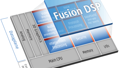
Cadence Design Systems, Inc. has announced the Cadence Tensilica Fusion digital signal processor (DSP) based on the 32-bit Xtensa Customizable Processor. The scalable DSP is aimed at applications requiring a microcontroller together with a DSP which can operate at ultra-low power levels and have a small footprint. It can be designed into SoCs for wearable activity monitoring, indoor navigation, context-aware sensor fusion, secure local wireless connectivity, face trigger, voice trigger and voice recognition. Optional Instruction Set Architecture (ISA) extensions are included to accelerate multiple wireless protocols including Bluetooth Low Energy, Thread and Zigbee using IEEE 802.15.4, SmartGrid 802.15.4g, Wi-Fi 802.11n and 802.11ah, 2G and LTE Category 0 release 12 and 13, and global navigation satellite systems (GNSS).
IoT device designers can configure just the options they need using the Xtensa Processor Generator to create an optimized Tensilica Fusion processor. Tensilica Fusion DSP configurable elements include:
Gerard Andrews, senior product manager with Cadence's audio/voice IP group, said: "Semico has predicted there will be 40 billion sensors a year by 2018, which means more data needs to be processed, cleaned, filtered and acted on. In most cases, the devices which will be doing this will be low cost, with low energy requirements."
IoT device designers can configure just the options they need using the Xtensa Processor Generator to create an optimized Tensilica Fusion processor. Tensilica Fusion DSP configurable elements include:
- Tightly integrated floating point
- 1-4 MACs supporting real and complex operations
- AES-128 encryption
- Flexible memory architecture
- MAC and PHY algorithm acceleration
- Audio/voice compatibility with the Tensilica HiFi architecture
Gerard Andrews, senior product manager with Cadence's audio/voice IP group, said: "Semico has predicted there will be 40 billion sensors a year by 2018, which means more data needs to be processed, cleaned, filtered and acted on. In most cases, the devices which will be doing this will be low cost, with low energy requirements."
Read full article
Hide full article