
AM DDS Function Generator
Want to build a DDS high performance function generator with the popular AD9834, BUT using a micro of your choice? Read on.
The AM DDS Function Generator
Introduction
The DDS Function Generator project by Theodorou Gerasimos in Elektor Nov/Dec 2015 certainly caught my attention! But as I examined the article I found he used an Analog Devices micro. Now Analog Devices makes superior components and I have no doubt their micros are excellent, but I didn't want to buy yet another micro and come up to speed on yet another tool set. So, I set out to extract the analog portion of the article above on a separate PCB that would interface to Any Micro (hence AM in the title). In this case since I had some on hand, my choice was the NXP MC9S12E128 supplied on a development board produced by Technological Arts. Not being a fan of the tiny cell phone graphic LCD's, this project will use a 4x16 character LCD; but the display is up to you. Similarly, the user input is via a 4x4 hex keypad, but you could use push buttons; the choice is yours. And best of all, the controller is your choice! Your controller will need a DAC and an ADC however, unless you want to make major changes.
Design Constraints
Having all the electronics on a narrow PCB that mounts vertically to the front panel is certainly a space saver. However my development board is too tall to mount vertically in the Hammond box for the original project. But those Hammond boxes look so good I wanted to stay with that style. The next longer box in that series might work for me?
I elected to use a power supply of my own construction. The power supply designed by Elektor wouldn’t fit in the Hammond box along with the other circuitry and components or I would’ve used it. Fortunately I was able to find a Hammond transformer with adequate specs that wasn’t too tall. So I was able to keep the power supply and heatsink well to the back of the box leaving adequate room for the new analog board as well as the micro board. These are both attached to a mother board which contains the power supply.
The Analog PCB
Given the size of the development board I planned to use and the size of the other parts I was able to make a good estimate of the available space for the analog PCB. So after drawing a schematic of just the analog components the PCB design could begin. The analog PCB matches the analog circuitry from the original project; no circuit changes were made and the component numbering matches the original. However some connectors are required for signals from the micro, power and pots. Connectors for the LCD and keypad are on the mother board. The schematic for the analog board is shown in the Design Spark file AM DDS Analog.sch contained in the attached zip file. And the Design Spark PCB layout can be seen in AM DDS Analog.pcb.
When the PCB was done I saw that I could’ve made it smaller. Maybe next time. What was important was did it actually work? The finished but unpopulated PCB is shown in AM DDS Analog.jpg which is attached.
The Mother Board
Before the analog board could be tested the mother board had to be completed. This meant mounting the micro and the analog board. Also connectors and wiring is needed for pots, power and micro connections. The Design Spark schematic of the mother board is AM DDS Mother.sch in the attached zip file. A top view of the mother board with the 9S12 and the analog board installed can be seen in AM DDS Mother.jpg. In that photo there are 2 14 pin dip sockets that are empty; these are for the LCD and keypad. Initial testing was done without the LCD or keypad.
Testing the Analog PCB
Getting a project like this to work is always a challenge. The circuitry may or may not work. Before you can test the circuitry you need to write some code. The code may or may not be correct. I was stuck in this loop for some time. Let me explain.
In order test the AD9834 you need to be able to communicate with it. The interface to the micro is via an SPI link. This should be easy I thought. I have used the SPI on the 9S12 before as well on other micros. Using the data sheet as a guide I set up the SPI. Although it seems to be doing things right I get no response from the AD9834. Read the data sheet some more. I find a discrepancy re the SPI set up. Try that; still doesn’t work. Then as a last resort I try all other SPI combinations; still doesn’t work. Out of utter desperation I tried bit-banging the SPI. It worked! I’m still not sure why the 9S12 SPI wouldn’t work. I may go back and examine that again sometime. So I finally got the AD9834 to produce a waveform of the desired frequency. This meant that I could now go on and test the remaining analog portion of the project.
Because I wished to eliminate all possible sources of trouble, no testing was done without everything being connected. Normally op amps just saturate when the inputs are left open, but I didn’t want to risk trouble here. So, the pots were connected for testing. Also the DAC was made to provide an output voltage for preliminary testing. Soon I was able to show that all parts of the analog board worked as desired.
So the layout of the analog board was correct in that all the circuitry was working as expected. There was one minor error. The BNC connector pinout assumed the connector would be on the bottom of the PCB, but it was mounted on the top here. This was a minor inconvenience with an easy workaround. So now the development of the project code can begin.
Code for the AM DDS Function Generator
The code for the original project was used as a guide here. However, the 2 projects are different enough that little copying was possible. I’ll outline some of the major differences here.
The method I use for calculating the number to send to the AD9834 is different. Since I chose to not incorporate a sweep feature, frequency numbers do not have to be calculated often. So there was no reason to avoid using floating point math.
I had trouble following the method used in the original project to calculate the output voltages from the sampled data, so I did it my own way. Although I did not go to lengths to explain what I did in my code I developed a document that explains my method quite clearly. This document is The Interface Circuit Analysis.docx and is attached.
Similarly, I dealt with the square wave duty cycle differently. In doing so I developed a document that analyzes the Schmitt Trigger circuit that produces the variable duty cycle square wave. See Square Wave Duty Cycle Analysis.docx which is attached. This analysis results in an expression defining the relationship between duty cycle and ADC count. With that relationship a look-up table was constructed which allows duty cycle to be selected by specifying an index into the table.
I had 2 reasons for choosing a character display and a keypad for user IO. Since have used this combination in other projects, I have code that works; this helps shorten the development time. Also, I preferred to have the IO on the top of the project where it’s easy to see. If the unit was to be used up on a shelf then my choice may not be the best one.
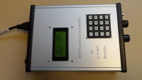
It took quite a while to get all the code to work properly, but eventually I had a functioning DDS function generator. The finished unit is shown in AM DDS Function Generator.jpg which appears on the banner. The code for this project is included as AM DDS Code.zip.
Source for the Adapt9S12E128 development board:
http://www.technologicalarts.ca/shop/store/category/21/microcontrollers/9s12.html
Introduction
The DDS Function Generator project by Theodorou Gerasimos in Elektor Nov/Dec 2015 certainly caught my attention! But as I examined the article I found he used an Analog Devices micro. Now Analog Devices makes superior components and I have no doubt their micros are excellent, but I didn't want to buy yet another micro and come up to speed on yet another tool set. So, I set out to extract the analog portion of the article above on a separate PCB that would interface to Any Micro (hence AM in the title). In this case since I had some on hand, my choice was the NXP MC9S12E128 supplied on a development board produced by Technological Arts. Not being a fan of the tiny cell phone graphic LCD's, this project will use a 4x16 character LCD; but the display is up to you. Similarly, the user input is via a 4x4 hex keypad, but you could use push buttons; the choice is yours. And best of all, the controller is your choice! Your controller will need a DAC and an ADC however, unless you want to make major changes.
Design Constraints
Having all the electronics on a narrow PCB that mounts vertically to the front panel is certainly a space saver. However my development board is too tall to mount vertically in the Hammond box for the original project. But those Hammond boxes look so good I wanted to stay with that style. The next longer box in that series might work for me?
I elected to use a power supply of my own construction. The power supply designed by Elektor wouldn’t fit in the Hammond box along with the other circuitry and components or I would’ve used it. Fortunately I was able to find a Hammond transformer with adequate specs that wasn’t too tall. So I was able to keep the power supply and heatsink well to the back of the box leaving adequate room for the new analog board as well as the micro board. These are both attached to a mother board which contains the power supply.
The Analog PCB
Given the size of the development board I planned to use and the size of the other parts I was able to make a good estimate of the available space for the analog PCB. So after drawing a schematic of just the analog components the PCB design could begin. The analog PCB matches the analog circuitry from the original project; no circuit changes were made and the component numbering matches the original. However some connectors are required for signals from the micro, power and pots. Connectors for the LCD and keypad are on the mother board. The schematic for the analog board is shown in the Design Spark file AM DDS Analog.sch contained in the attached zip file. And the Design Spark PCB layout can be seen in AM DDS Analog.pcb.
When the PCB was done I saw that I could’ve made it smaller. Maybe next time. What was important was did it actually work? The finished but unpopulated PCB is shown in AM DDS Analog.jpg which is attached.
The Mother Board
Before the analog board could be tested the mother board had to be completed. This meant mounting the micro and the analog board. Also connectors and wiring is needed for pots, power and micro connections. The Design Spark schematic of the mother board is AM DDS Mother.sch in the attached zip file. A top view of the mother board with the 9S12 and the analog board installed can be seen in AM DDS Mother.jpg. In that photo there are 2 14 pin dip sockets that are empty; these are for the LCD and keypad. Initial testing was done without the LCD or keypad.
Testing the Analog PCB
Getting a project like this to work is always a challenge. The circuitry may or may not work. Before you can test the circuitry you need to write some code. The code may or may not be correct. I was stuck in this loop for some time. Let me explain.
In order test the AD9834 you need to be able to communicate with it. The interface to the micro is via an SPI link. This should be easy I thought. I have used the SPI on the 9S12 before as well on other micros. Using the data sheet as a guide I set up the SPI. Although it seems to be doing things right I get no response from the AD9834. Read the data sheet some more. I find a discrepancy re the SPI set up. Try that; still doesn’t work. Then as a last resort I try all other SPI combinations; still doesn’t work. Out of utter desperation I tried bit-banging the SPI. It worked! I’m still not sure why the 9S12 SPI wouldn’t work. I may go back and examine that again sometime. So I finally got the AD9834 to produce a waveform of the desired frequency. This meant that I could now go on and test the remaining analog portion of the project.
Because I wished to eliminate all possible sources of trouble, no testing was done without everything being connected. Normally op amps just saturate when the inputs are left open, but I didn’t want to risk trouble here. So, the pots were connected for testing. Also the DAC was made to provide an output voltage for preliminary testing. Soon I was able to show that all parts of the analog board worked as desired.
So the layout of the analog board was correct in that all the circuitry was working as expected. There was one minor error. The BNC connector pinout assumed the connector would be on the bottom of the PCB, but it was mounted on the top here. This was a minor inconvenience with an easy workaround. So now the development of the project code can begin.
Code for the AM DDS Function Generator
The code for the original project was used as a guide here. However, the 2 projects are different enough that little copying was possible. I’ll outline some of the major differences here.
The method I use for calculating the number to send to the AD9834 is different. Since I chose to not incorporate a sweep feature, frequency numbers do not have to be calculated often. So there was no reason to avoid using floating point math.
I had trouble following the method used in the original project to calculate the output voltages from the sampled data, so I did it my own way. Although I did not go to lengths to explain what I did in my code I developed a document that explains my method quite clearly. This document is The Interface Circuit Analysis.docx and is attached.
Similarly, I dealt with the square wave duty cycle differently. In doing so I developed a document that analyzes the Schmitt Trigger circuit that produces the variable duty cycle square wave. See Square Wave Duty Cycle Analysis.docx which is attached. This analysis results in an expression defining the relationship between duty cycle and ADC count. With that relationship a look-up table was constructed which allows duty cycle to be selected by specifying an index into the table.
I had 2 reasons for choosing a character display and a keypad for user IO. Since have used this combination in other projects, I have code that works; this helps shorten the development time. Also, I preferred to have the IO on the top of the project where it’s easy to see. If the unit was to be used up on a shelf then my choice may not be the best one.
It took quite a while to get all the code to work properly, but eventually I had a functioning DDS function generator. The finished unit is shown in AM DDS Function Generator.jpg which appears on the banner. The code for this project is included as AM DDS Code.zip.
Source for the Adapt9S12E128 development board:
http://www.technologicalarts.ca/shop/store/category/21/microcontrollers/9s12.html
Updates from the author