
Buffer Board for the Raspberry Pi 400
on
Released in November 2020, the Raspberry Pi 400 is actually a Raspberry 4, but built into a keyboard, with the GPIO expansion connector on the back of the enclosure. Connecting additional hardware always brings risks, especially during prototyping. The buffer board we present here is especially designed for the Raspberry Pi 400. It allows interfacing with both 3.3 V and 5 V external logic for all the 26 GPIOs, and the buffers/level shifters used for this also provide ESD protection.
The 400
Raspberry Pi boards will hardly need any introduction here. Since the introduction of the first version in 2012, they have been the subject (or part of) many projects in Elektor magazine. We have presented quite a few different hardware projects and extension PCBs for these processor boards. For this project, let’s spoil the suspense right away: the circuit I will cover is not new, as its first version was discussed back in 2015 an Elektor Labs page. In 2018, the design was adapted to the expanded, 40-pin I/O connector that has been the standard for connecting additional hardware to these processor boards since the introduction of the Raspberry Pi B+. And now, the latter version is adapted to one of the more recent members of the Raspberry Pi product family — the Raspberry Pi 400.
Very simply put, the 400 is a Raspberry 4, built into a keyboard. It resembles the once-famous computers of the 1980s, like the Commodore 64, Sinclair Spectrum, Acorn BBC and similar. In terms of specifications, the Raspberry Pi is of course many times more powerful than its now antique predecessors, but there is also a striking similarity — the GPIO expansion connector on the back of the enclosure, to which the user can connect external (self-designed) hardware. Connecting additional hardware always brings risks, especially during prototyping, and the buffer board presented here prevents the Raspberry Pi from being damaged in the process. In addition, the buffer board enables interfacing with both 3.3 V and 5 V external logic, and the buffers/level shifters used for this also provide ESD protection.
Hardware
The project’s schematic (Figure 1 and attached as download) is exactly the same as the one from our publication in 2018. The TXS0108E 8-bit buffers/voltage translators used in this project are bidirectional, and each A-port and B-port pin has a pull-up resistor. The pull-down resistor of a GPIO of the Raspberry Pi is typically in the order of 40 to 60 kΩ. This value is too high to properly pull-down the I/O when the buffer board is plugged in. So, please note that with this input configuration the logic level will not be low; the pull-down will not work as intended.
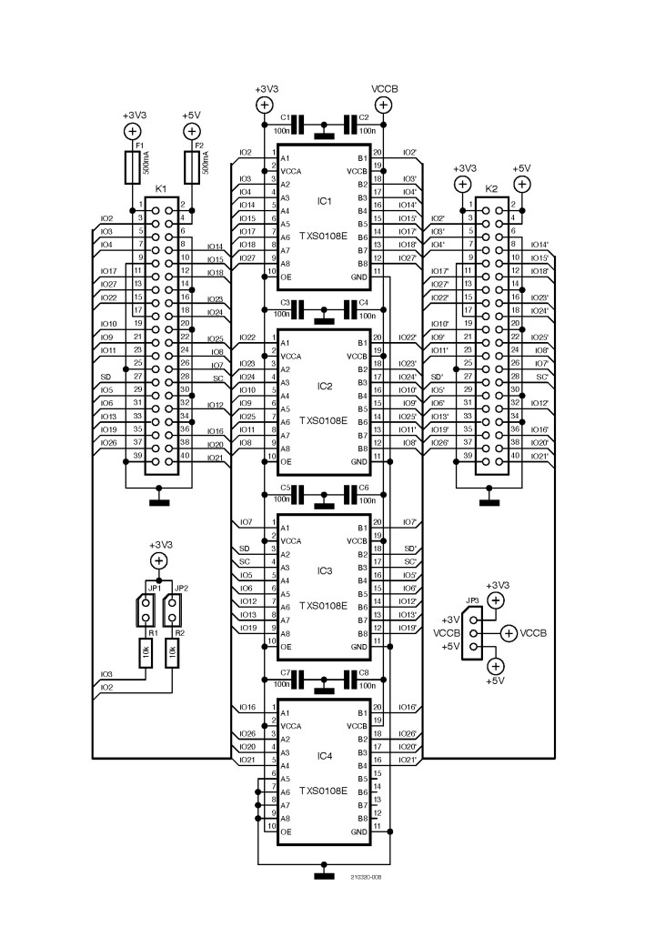
The I/Os have separate power supply pins for the Raspberry Pi side and the outside-world, VCCA and VCCB, respectively. Every A-port I/O of the TXS0108E has a pull-up resistor to VCCA, connected to the +3.3 V power supply of the Raspberry Pi 400, and each B-port I/O has a pull-up resistor to VCCB. VCCB — for the level of the I/Os on K2 — can be set to either +3.3 V or +5 V logic by jumper JP3. The pull-ups of the buffers have a value of 40 kΩ when the output is driving low and a value of 4 kΩ when the output is driving high. So the outputs of the buffers are in fact open drain. If, for instance, an LED is connected from the output of the buffer to ground, a voltage divider is created when an extra series resistor is used. A resistive load on the output will cause the logic high level to drop. Something to keep in mind!
There are two 0.5 A PPTC resettable fuses (F1 and F2) in the power connections between K1 to K2 on the buffer board to protect the +5 V and +3.3 V power supplies of the Raspberry Pi 400.
For the implementation of an I2C bus to communicate with external hardware, GPIO2 is SDA and GPIO3 is SCL, extra pull-up resistors R1 and R2 can be enabled by jumpers JP1 and JP2.
During boot of the Raspberry Pi GPIO0 (ID_SD) and GPIO1 (ID_SC) are used to read an EEPROM of an I2C HAT (Hardware Attached on Top). After boot-up these GPIO’s can be used like the 26 others, but care needs to be taken if an I2C HAT is mounted the system isn’t affected. To prevent the reading of GPIO0 and GPIO1 during boot add the following entry to /boot/config.txt:
force_eeprom_read=0
For more information, look at the Raspberry Pi documentation about the config.txt file.
The Printed Circuit Board
The schematic may be old news, but the PCB (Figure 2) is adapted especially for the Raspberry Pi 400. It’s a bit smaller than the original buffer board presented in 2018. The Gerber files for this new board are available for download, so you can order it at the PCB manufacturer of your choice. But it is, of course, a lot more convenient to buy the completely assembled buffer board in the Elektor Store.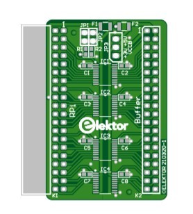
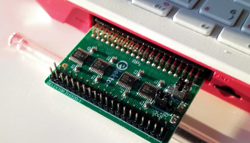
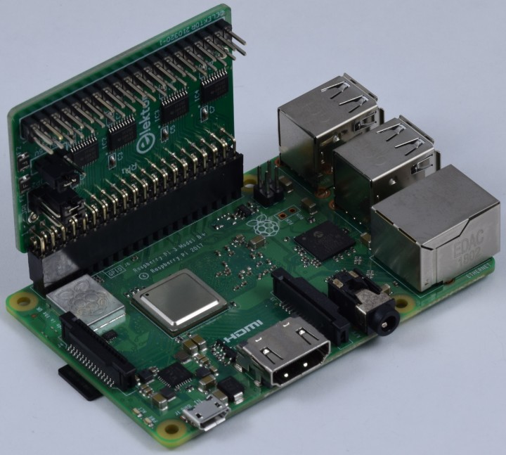
A right-angled receptacle is used for the connector on the Raspberry Pi 400 side of the buffer board (K1) so it can be inserted in the GPIO header in the back of the enclosure (Figure 3). The connector for the buffered I/Os is a standard 40-pin male vertical header (K2). The size of the module is 55 x 44 mm, including receptacle K1, which protrudes over the edge of the PCB. Compared to the original 150719-1 PCB, the two rows of pins of K1 are swapped, because a receptacle is used here. Placing a standard vertical male 40-way pin header for K1 to connect this buffer board to a Raspberry Pi 2, 3 or 4 via a flatcable — like with the older version of the buffer — will not work here.
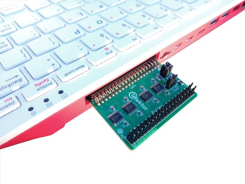
However, Figure 4 shows that this module can still be used with a Raspberry Pi 2, 3, or 4.
The output connector K2 can be connected to external circuits using a short 40-way ribbon cable with two 2 x 20 receptacle connectors attached, or just a single receptacle with short wires soldered to them or single sockets with wires. But be careful pressing a 40-way receptacle onto K2 or unplugging it from the board. Don’t do this while the buffer board is still inserted in the Raspberry Pi 400, because quite some force is needed and the Raspberry Pi 400’s GPIO header could get damaged.
Testing the Buffer Board
Two very simple Python programs for testing the buffer board – borrowed from the older project - are available for download at the Elektor Labs page of this project. One is to test all GPIOs as output, Check_all_GPIOs_as_output.py, and the other is to test all GPIOs as input, Check_all_GPIOs_as_input.py (210320-11.zip). In Raspbian, just double click on one of the files and the default IDE for Python will open, then select RUN to start the test.
When testing the GPIOs as output, only a single low-current LED connected between a pin and GND is needed to see if an output is working or not. As a series resistor for the LED a 1.8 kΩ resistor can be used, but the value is not really critical. It will limit the current through the LED if it is directly connected to the positive supply voltage. Outputs are sequentially tested in four groups of maximum eight pins each, named IOA to IOD. Because of the open drain output the voltage across an LED (red) plus resistor is about 2.6 V, when 5 V is selected as a power supply for the outputs (JP3). Connect the resistor plus LED to one of the selected outputs and it will be switched on for 0.2 seconds. The repetition rate of this pulse depends on the size of the group: 1.6 seconds for groups A to C (each with eight outputs) and only 0.4 seconds for group D (two outputs). Change ‘IOA’ to one the other groups in the line
for i in IOA: # leds blink 0.2 s in IOx group
to test the other groups of outputs. Of course, GPIO0 and GPIO1 (ID_SD and ID_SC) can be added to one of the groups too.
The program to test the GPIOs as input uses one I/O as output to indicate that the input under test is working, GPIO3 by default. Connect a 1.8 kΩ resistor and LED between pin 5 (IO3’) of K2 and GND. Only one input at a time is tested in the source code, to make sure only this one is working as input. Change the number in the following line to test another GPIO as input:
IN1 = 2 #selected GPIO to test as input
The program also prints the selected GPIO and its input level. The inputs have their pull-ups enabled. So to make the connected LED light the current input pin must be connected to ground. When done so the printout will change. Finally, select a different GPIO for the output so you can also check GPIO3 as input. Of course, there are numerous ways to test the GPIOs, if anyone has a more efficient and/or faster way: please share.
This buffer allows you to connect new hardware to the Raspberry Pi 400 with peace of mind, greatly reducing the chance of it getting damaged during experiments. But still, reducing the risk by using this buffer board doesn’t mean that nothing can go wrong. In many cases, I won’t hurt to add some common sense too.
Questions About the Buffer Board?
If you have technical questions or comments about the buffer board or this article, feel free to e-mail the Elektor editorial team at editor@elektor.com.
Discussion (0 comments)