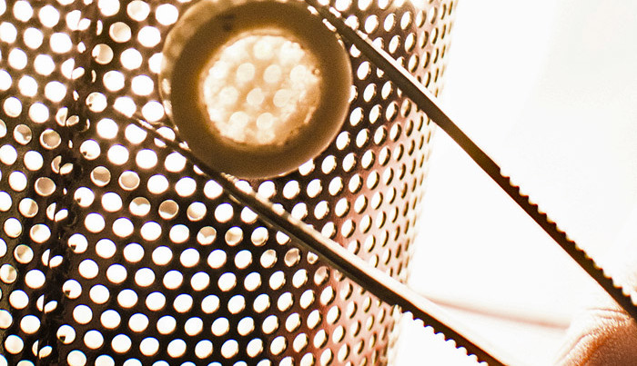
Laser welded transparent ceramic cylindrical cap assembly. Image: Garay Lab.
A new ceramic welding technique developed by a team of engineers at the University of California San Diego could soon be making tough scratch-resistant Smartphones, non-metallic pacemaker implants and robust enclosures suitable for protecting electronics in harsh environments...
Bonding ceramic materials by welding usually requires a furnace to achieve the necessary high temperature. A new technique using an ultrafast pulsed laser to melt and join together ceramic materials along the interface is described in an article published in the journal Science. The process can be carried out in normal environmental conditions and uses less than 50 watts of laser power.
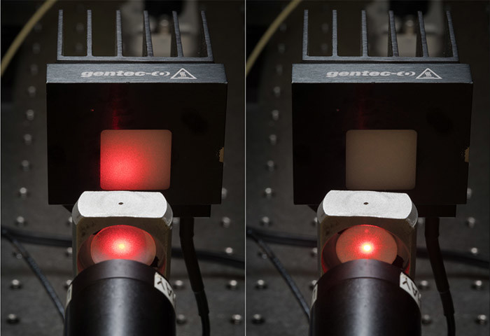
Welding ceramic work pieces successfully has been a fundamental challenge as it requires very high temperatures and the extreme temperature gradients produced can easily cause the material to crack. Ceramics are of great interest because they are biocompatible, extremely hard and unbreakable, making them ideal for use with biomedical implants and as enclosures for electronic systems. However, the methods used currently for bonding makes their use impractical. Optical transmission through a transparent ceramic (left) and a conventional opaque ceramic material (right).
Images by David Baillot, UCSD Jacobs School of Engineering.
Pulses are the key
The solution is to deliver a series of short laser pulses along the join between two ceramic parts so that the heat is applied locally to form a pool of molten ceramic. For this to be successful its necessary to carefully control the laser parameters (exposure time, number of laser pulses and pulse duration) and the transparency of the ceramic material. With the right combination, the laser energy is easily absorbed, so that welds with relatively low laser power of <50 W can be performed at room temperature.
Tests showed that 2 ps pulses at a repetition rate of 1 MHz with a moderate total number of pulses was ideal. The diameter of the melt is maximized and material ablation is minimized. In addition, no extreme temperature gradients occur over the entire work piece and cooling is fast.
To test the technique researchers welded a transparent cylindrical cap to the inside of a ceramic tube. The welded tube successfully withstood subsequent vacuum testing. Tests like this are used in industry to validate gaskets on electronic and optoelectronic devices. So far, this new welding technique has only been used with small ceramic parts <2 cm. The process is currently being optimized for larger scale use as well as for different material types and geometries.
Elektor Magazine has been one of the leading sources of information on electronics for engineers, designers, start-ups and companies for 65 years. Our magazine is powered by an active community of electronics engineers – from students to professionals – who are passionate about designing and sharing innovative ideas.
For them, we publish hundreds of items a year, in formats such as articles, videos, webinars, and other learning formats. Our mission is to share knowledge in every possible way and inspire readers with the latest developments within the electrical engineering sector.
Thank you for your vote!
Leave further comments in the fields below.
Thank you for your vote!
If you wish to leave a comment with your rating, please first use the login below. If not, just close this window.

Discussion (0 comments)