
High-Voltage-Power-Insulated-SSR: Embed Your Own Solid-State Relay in Your Projects
on
Solid-state relays, also known as SSRs, are widely available on the market, for any voltage or current rating. Why make one, then? Because it is sometimes useful, in terms of cost-effectiveness and PCB space constraints, to incorporate one right into our circuit. In this article, we’ll see how to design it with discrete components.
Nowadays, an increasing number of circuits are utilizing MOSFETs to switch high currents and voltages. This advancement has been made feasible by construction technologies that enable the production of transistors suitable for a wide range of voltages and currents. These transistors can handle tasks once exclusively managed by thyristors and power relays. There are various circuit configurations for creating solid-state switches based on MOSFETs. In this article, we will explore the commonly used configurations and propose an application for a series switch. This switch is controlled through a circuit that is electrically isolated from the one being sectioned.
To grasp the intricacies of this application, we should begin with some foundational theory. As shown in Figure 1, to operate an N-channel enhancement-type MOSFET, it suffices to drive its gate with a voltage pulse relative to the source, which serves as the common terminal. The drain then switches the current into the load. In this scenario, the load is connected between the positive supply and the drain terminal itself.
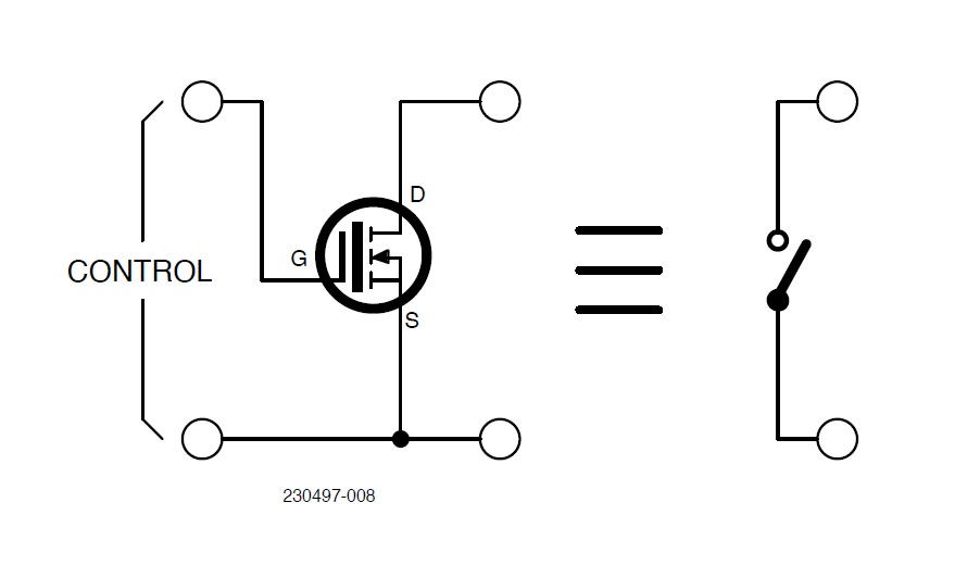
When the gate is positively biased relative to the source, the MOSFET enters a conductive (or “on”) state. In this state, the resistance between the drain and source can drop to just a few tens of milliohms. Conversely, if the gate is isolated or connected to the source through a resistor or a short-circuit, the transistor enters a non-conductive (or “off”) state. In this off state, the resistance between its drain and source is theoretically infinite, but in practical terms, it ranges from tens of megohms to gigaohms. To initiate conduction in the MOSFET, the potential difference between the gate and source must exceed the threshold potential.
The schematic depicted in Figure 1 may not always be ideal, particularly because it necessitates that the source is shared between the “switch circuit” and the “control circuit.” This shared configuration can be problematic in situations where the ground of the control circuit and the power circuit are at different potentials, or when the switch needs to be floating — such as having a terminal connected to the positive power supply. In these instances, the design falls short and an alternative approach is required. The design outlined in this article offers a solution to this challenge. While not widely used, it is both simple to implement and cost-effective.
Isolated Command: Options
The two most commonly used methods for transferring a condition between two circuits while maintaining galvanic isolation are:
- Magnetic isolation (transformer);
- Optical isolation (opto-couplers, opto-batteries, fiber optics);
Magnetic isolation, often achieved through a transformer, is perhaps the most well-known method. However, it is widely recognized that this method cannot sustain the conduction condition indefinitely. This limitation arises because a transformer only functions with flux changes. Therefore, if one needs to keep the MOSFET in an “on” state for extended periods, magnetic isolation would not be suitable. Transformer isolation might be a good choice when the MOSFET is required to switch continuously, or if it needs to remain mostly in the “off” state and only switch to conduction briefly (as in an impulse command).
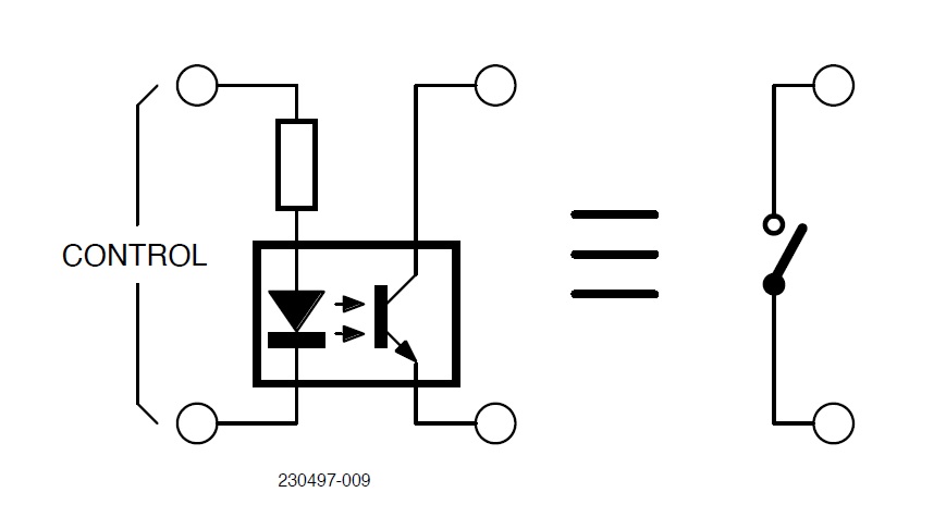
Isolation achieved using a photo-coupler is indeed “galvanic.” On one side of the photo-coupler, the emitter diode is driven by the voltage of the control circuit. This emitter diode then illuminates the output photo-transistor, causing it to go into saturation. Figure 2 shows the traditional optical coupling scheme. In our project, we utilize this type of coupling.
To use a photo-coupler for transferring the gate command to the MOSFET, it’s necessary to have a supply voltage on the output side as well. This supply voltage is what the photo-transistor will switch to turn the MOSFET on. The circuit solution for this setup is depicted in Figure 3.
The Circuit
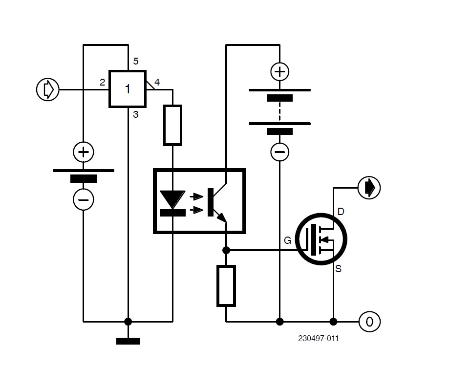
As you can see in the schematic of Figure 4, we have developed a solution that eliminates the need for a power supply, thanks to a specific integrated circuit. This solution essentially involves the use of LEDs, an optical channel, and a photovoltaic cell connected at the bottom of the optical channel. When the LED illuminates the cell, it generates a voltage high enough to surpass the gate-source threshold voltage of the power MOSFET, which is used as a static switch.
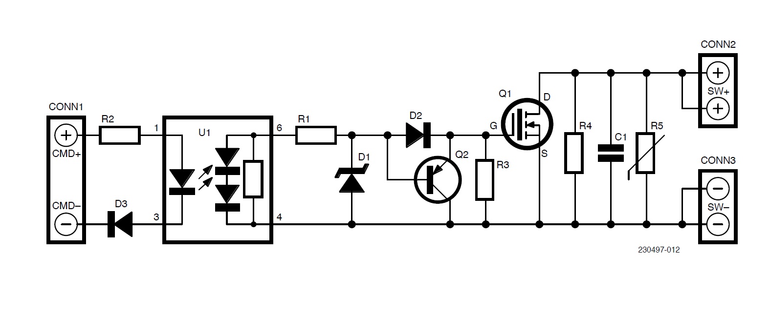
Fortunately, there’s an integrated version of this assembly, often referred to in various ways, but which we might consider a “PV element” — the TLP3906 is one such example. You can think of it as similar to a classic photocoupler, but instead of a phototransistor, it has an array of photovoltaic cells connected in series. If you would like to learn more about this, see the relevant datasheet that can be found on the manufacturer’s website.
Having considered this, we can think of it as connecting the output of the TLP3906 directly to the gate and source terminals of the power MOSFET, resulting in a control of the MOSFET that is completely isolated from the control circuit. The TLP3906 has an isolation of 3,750 V, so it’s suitable for many cases of practical interest. Of course, the connection of the TLP3906 to the power MOSFET requires some care. So let us take a look at the circuit diagram: we note the control connector (CONN1) on which a voltage of 5 V will have to be applied to cause the MOSFET to go on and a voltage of 0 V to cause its interdiction. This will result in the SW+ (CONN2) and SW- (CONN3) terminals being shorted or open, respectively.
The “control” side of the circuit includes a current-limiting resistor R2 and a protection diode D3. These components are crucial for preventing stress on the TLP3906 in case the CONN1 connector terminals are connected in reverse. This section of the circuit is designed to properly power the emitter diode of the TLP3906. The resistor R2 is calibrated for a 5 V input, but it can be adjusted (as discussed later in the text) to accommodate control input voltages ranging from 3.3 V to over 28 V.
Downstream of the TLP3906, and before the gate and source terminals of the power MOSFET, there's a simple circuit composed of R1, D1, D2, Q2, and R3. This circuitry optimizes the control of the MOSFET. Resistor R1 and Zener diode D1 together form a basic protection mechanism for the TLP3906, which is especially useful in guarding against voltage transients on the power side that might affect this component. Although this protection might be unnecessary in most cases, given its modest cost, it is considered beneficial to include it.
Components R3, D2, and Q2 are essential for accelerating the MOSFET’s turn-off phase and counteracting the issue posed by the large parasitic capacitance between the MOSFET's gate and source terminals. This parasitic capacitance is inherent to the physics of the device, and is particularly prominent in transistors designed to withstand high voltages and currents. Consequently, when the MOSFET is brought into conduction by the voltage generated by the TLP3906, it accumulates a significant charge on its gate-source capacitance. This charge can linger for an extended period when the TLP3906 ceases supplying voltage.
The primary concern with this situation is not just the delay in turning off the MOSFET after disengaging the control, but also the fact that, without appropriate measures, the transition from a conducting to an open state would occur gradually, akin to a capacitor discharging through a high-value resistor. Such a slow transition from conduction to non-conduction could lead to extremely high-power dissipation in the MOSFET, potentially causing damage. It’s crucial to implement these components to ensure a swift and safe transition for the MOSFET from the conducting to the non-conducting state.
What is desired instead, in all switching circuits, is a smooth transition between one state and the other. The circuit consisting of R3, D2 and Q2 performs just this task: when voltage is supplied by the TLP3906, the base of Q2 (PNP) is at a higher potential than that of the emitter and therefore Q2 is interdicted, so it doesn’t affect the gate and source terminals of the MOSFET.
However, when the TLP3906 stops supplying power, the base of Q2 will be at a potential close to that of the collector, driving it into the on state. As a result, the charge stored in the MOSFET’s parasitic gate-source capacitance is rapidly discharged through the collector and emitter terminals of Q2. This rapid discharge ensures the fast transition from the conducting to the non-conducting state in the MOSFET, which is precisely what we aim for in an efficient switching circuit.
In the opposite transition, the speed of the latter is ensured by the current that the TLP3906 can provide and which can charge the gate-source parasitic capacitance reasonably quickly. The values found on the prototype are 400 µs for the transition time from interdiction to conduction states, and 14 µs for the opposite transition, from conduction to interdiction, using a type STWA12N120K5 MOSFET, capable of withstanding 1,200 V and 12 A while showing a resistance of about 0.7 Ω. Having other requirements for voltage and current to be switched, a wide variety of power MOSFETs can be used, ensuring similar switching times. As mentioned above, in case a switching voltage other than 5 V is desired, it will be necessary to change the value of R2 as per the following formula:
R2 = (Vcmd - 2.2) / 0.012
and choose the nearest commercial value. For example, for a voltage of 3.3 V a value of 100 Ω will be used for R2, while 820 Ω will be needed for 12 V and 1,800 Ω for 24 V. Three components, C1, R4 and R5, are inserted between the CONN1 and CONN2 connectors of the power circuit, with the function of damping surges (snubber circuit) that may occur upon switching loads of a certain magnitude.
Resistor R4 allows multiple static switches to be put in series, causing the voltage to distribute equally when the MOSFET is open. R5 is a varistor capable of suppressing fast transients, and C1 helps it in this task.
Practical Realization
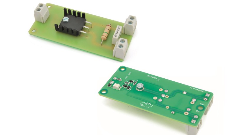
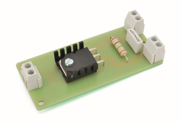
The circuit consists of some surface-mount and some conventional-mount components. The power MOSFET is through-hole type, while the TLP3906 exists only surface-mount, so all components around the TLP3906 were also provided surface-mount. The snubber components are through-hole, given the large currents and/or voltages they must be able to withstand (Figure 5). The PCB was provided for MOSFETs in TO-247 and TO-220 packages: for the latter, it will be necessary to spread the outer pins slightly, given the smaller pitch.
In making the PCB, we have taken certain precautions: the control part has been kept well separated (and on the opposite face of the PCB) from the power part; the latter has the tracks connecting drain and source to their respective terminals, sized to carry all the current expected during operation and isolated from each other and those of the other components so as to withstand the voltages involved. There are precise standards for sizing the tracks according to these requirements; the circuit board was designed to withstand more than 10 A and provide more than 1 kV isolation. It has been tested under such conditions successfully.
Component List
| Resistors | Capacitor | Semiconductors | Miscellaneous |
| R1 = 1 kΩ (1206) | C1 = 1 nF, 1 kV, ceramic, pitch 15 mm | Q1 = STWA12N120K5 | 3 × 2 Poles Screw Terminal Block, pitch 5.08 mm |
| R2 = 270 Ω (1206) | Q2 = BC807 | 1 × Heat Sink | |
| R3 = 1 MΩ (1206) | D1 = MMSZ5248B | 1 × 3 MAx12 Screw | |
| R4 = 1 MΩ 2W (T.H.) | D2 = BAV70 (SOT23) | 1 × 3 MA Nut with washer | |
| R5 = Varistor S20K (T.H.) | D3 = BAV70 (SOT23) | 1 × S1340 PCB (84 x 38 mm) | |
| U1 = TLP3906 |
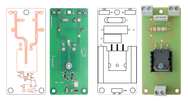
As described in the previous paragraphs, it is necessary to mount some components on one side of the PCB and others on the opposite side. A good rule of thumb is to mount the lowest profile (i.e., height from the surface of the PCB) components first, and then start with the SMDs. There are no particularly small components, but even a 1206 size resistor is about 3 × 1.5 mm, so it will have to be treated with care. We will start, then, by assembling resistors R1, R2 and R3 and then the two diodes D1, D2 and D3 to finish the first part with transistor Q2 first and opto-battery U1 then. For the latter there is no special attention, except that it is good to mount it last and be careful not to damage it in the later stages of board assembly and use, since it is the component most protruding on this side of the PCB At this point, we will go to the other side of the board and attach Q1 and its heatsink fin to the PCB by means of a M3 × 10 screw, with a nut and possibly a spring washer, after appropriately bending Q1 leads at 90° so that once inserted into the PCB the fixing hole will match accurately. No thermal conductive paste is needed between the heatsink and Q1. Once the leads of Q1 are soldered, you will taper them with the usual electronics cutters (with the cut “flush,” so as not to leave protrusions of the leads on the solder side).
Then we will mount the other three components (optional, see previous description) R4, R5, and C1 with the same procedure used for Q1 and all through-hole components. To complete the job, we will mount the three terminal blocks from PCB labeled CONN1, CONN2, and CONN3. You’ll have thus finished assembly and the circuit ready to operate, since it does not require calibration. The PCB layout files can be downloaded from here.
Commissioning
The first test will require only a multimeter on the Ohm range and a power supply capable of supplying a voltage of 5 V with a current delivered of about 10 mA. You will connect the positive lead of the multimeter on the CONN2 connector and the negative lead on the CONN3 connector. Without any other connection, the multimeter should indicate an open circuit. In the event a diode-like reading is given, it will mean that the positive tip of your multimeter will, in fact, be the one at lower potential when operating as an ohmmeter: this was common in the old pointer instrument multimeters available on the market over 20 years ago.
When you supply 5 V voltage to the terminals of the control connector CONN1, you should see the multimeter readout go to virtually zero. If it does not, in addition to rechecking for any assembly errors (or defective components, in case they were salvaged ones...) you will have to check that the polarity of the control voltage is correct. You can recognize pin 1 of the CONN1 connector on the PCB because it is the one with the square pad, and this is where the negative pole of the control voltage will need to be connected. At this point one can move on to tests closer to what is required by our application, taking care to start with gradually increasing voltages and currents and gradually verify that connection errors, bad soldering, or other problems typical of prototype assembly, and of “home” assembly in general, do not create problems. Such as, for example, overheating or sparking noise — the currents involved can be high with these MOSFETs!
Warning: High Voltage!
The MOSFET suggested for this project, a STWA12N120K5, is capable of withstanding 1200 V and 12 A: these values can be very dangerous!
Voltages above 50 V are considered “high voltage” for which a number of safety regulations must be applied that cannot be recalled in these pages. In any case, the things to know are that with voltages above a few hundred volts it is possible for surface discharges to start even where our common practice with 230 V systems tells us that there is no such risk. This is the case even if the circuit board is professionally made and assembled; worse still if there is solder residue, moisture or, worst of all, the test is carried out with the circuit board resting on the assembly table where bits of terminals, the tin wire and other conductors are still present! So testing will have to take place under absolutely safe conditions.
One of the things to be provided — even for the first tests — is an enclosure for the printed circuit board that eliminates the possible risks in case of failure of a component, in the case of the above-mentioned discharges, and for all the other risks and that these demanding electrical parameters can present. The enclosure also has the important function of protecting against the projection of molten material that can occur when the circuit connected to this switch is capable of supplying high currents (several tens of amperes) and a fault is created in the switch that results in a short circuit. In this unfortunate (but not impossible!) condition, the connections and circuit board tracks could melt in the short time of the short circuit and create a kind of small explosion, capable of projecting microscopic drops of molten metal that could still be capable of generating damage to property and people. So always exercise extreme caution and operate this switch only after placing it in an enclosure.
In any case, the circuit is sized to have only a slight rise in the temperature of the MOSFET operating at the maximum of the given parameters; all other components should remain at room temperature, given the minimal dissipation. Different is the case of repeated switching at very short times, but that is another matter; this situation could occur in the case of continuous switching at the frequency of a few kHz or more.
Connection Possibilities
First, it is worth mentioning that MOSFETs are capable of interrupting unipolar currents, as evidenced by the marking of the power terminals with SW+ and SW- for CONN2 and CONN3 connectors, respectively. This means that the SW+ terminal will necessarily have to be at higher potential than the SW- terminal, and current will have to flow from SW+ to SW-, or it will not function as a switch.
Choosing MOSFET's
The device (i.e., the MOSFET) type to be used to switch current depends mainly on the magnitudes (current and voltage) with which to operate. It will therefore be necessary to choose a component that can withstand the maximum current values that the project will require to circulate when the switch is closed (ON), and the maximum voltages present between drain and source when the switch is open (OFF). The printed circuit board allows the use of MOSFET in TO-220 and TO-247 packages. Even narrowing down to these two enclosures, MOSFET ranging from a few tens of volts as maximum voltage and a few amperes of maximum current, to over 1 kV and a few tens of amperes can be mounted. The proposed device is one that “demonstrates” the potential of the circuit, a kind of “dream car”: you may not need it, but it can go that far. For the choice of the most suitable component (and the one that is economically justifiable) one can turn to the online catalogs of MOSFET manufacturers; here, select the package, the minimum current for the application (keep a safety margin of at least 1.5:1), and the maximum voltage (same for the safety coefficient). The only caution that one will then have to place before the final choice of the component will be that related to the driving, considering that the TLP191B provides a gate voltage of about 10 V: one must be sure (and for this, it is essential to consult the datasheet) that with this voltage the MOSFET will be able to pass effectively to ON state. That is, feature a RDSon low enough for the application for which you are choosing it. Translating “low enough” into quantitative terms, means evaluating that the voltage drop across the MOSFET in conduction is acceptable for the purposes. And most importantly, that the power dissipation on the MOSFET is compatible with the device and the heat sink adopted. The power dissipation is calculated by the formula:
Pd=I2*RDSon
while Pdmax should be calculated from the thermal resistances of the device and the heat sink.
Power MOSFETs are internally equipped with a protection diode, with the cathode connected to the drain and the anode to the source. In this way, if the MOSFET is accidentally affected by a reversed voltage, it will be the diode that will always keep it in conduction, nullifying the switch capability! This feature, however, can be exploited to obtain a bipolar current switch. By making two identical prototypes of this design and connecting the SW- terminals of the two boards together, voltages of any polarity can be applied between the SW+ terminals, with a little care. The aforementioned protection diode inside the MOSFET may not continuously withstand all the current it will be interested in, so it will be advisable to consult the datasheet of the MOSFET to verify this possibility of use.
As an alternative, a higher power diode can be applied externally and, possibly, with a heat sink. In this configuration, the control to the two prototype boards will have to be identical: therefore, the two CONN1 terminal blocks will have to be connected in parallel. As mentioned in the description of operation, it will be possible to connect multiple switches in series by making multiple boards of the same circuit and by connecting the SW+ terminal of one to the SW- of the next and having the extreme SW+ and SW- terminals available for the circuit to be switched; again, the CONN1 terminal blocks should all be connected in parallel. Keep in mind that the TLP3906 guarantees isolation up to 3,750V; remember, however, that if you go as far as that voltage (but even to half that...) extreme care is required in working around the circuit, which will have to be well isolated from any surrounding metal parts and wiring and which should not be approached unless the voltage is disconnected!
Final Considerations
The circuit lends itself to various applications, as well as can be a starting point for similar realizations. The TLP3906 can also be used for other purposes, not necessarily in power circuits or for driving MOSFETs: it is an interesting component that deserves some experimentation, depending on one’s imagination. Caution is still recommended if the circuit is to be used in applications where high currents and especially high voltages are present.
Editor’s notes: Interested in ESP32 and DIY projects? This project originally appeared in Elettronica IN.
Discussion (0 comments)