
The Future of Inkjet-Printed Electronics
January 29, 2014
By Benjamin Cook
Over the past decade, major advances in additive printing technologies in the 2-D and 3-D electronics fabrication space have accelerated additive processing—printing in particular—into the mainstream for the fabrication of low-cost, conformal, and environmentally friendly electronic components and systems. Printed electronics technology is opening an entirely new world of simple and rapid fabrication to hobbyists, research labs, and even commercial electronics manufacturers.
Historically, PCBs and ICs have been fabricated using subtractive processing techniques such as photolithography and mechanical milling. These traditional techniques are costly and time-consuming. They produce large amounts of material and chemical waste and they are also difficult to perform on a small scale for rapid prototyping and experimentation.
To overcome the limitations of subtractive fabrication, over the past decade the ATHENA group at the Georgia Institute of Technology (Georgia Tech) has been developing an innovative inkjet-printing platform that can print complex, vertical ICs directly from a desktop inkjet printer.
To convert a standard desktop inkjet printer into an electronics fabrication platform, custom electronic inks developed by Georgia Tech replace the standard photo inks that are ejected out of the printer’s piezoelectric nozzles. Inks for depositing conductors, insulators/dielectrics, and sensors have all been developed. These inks can print not only single-layer flexible PCBs, but they can also print complex, vertically integrated electronic structures (e.g., multilayer wiring with interlayer vias, parallel-plate capacitors, batteries, and sensing topologies to sense gas, temperature, humidity, and touch).
To create highly efficient electronic inks, which are the key to the printing platform, Georgia Tech researchers exploit the nanoscale properties of electronic materials. Highly conductive metals (e.g., gold, silver, and copper) have very high melting temperatures of approximately 1,000°C when the materials are in their bulk or large-scale form. However, when these metals are decreased to nanometer-sized particles, their melting temperature dramatically decreases to below 100°C. These nanoscale particles can then be dispersed within a solvent (e.g., water or alcohol) and printed through an inkjet nozzle, which is large enough to pass the nanoparticles. After printing, the metal layer printed with nanoparticles is heated at a low temperature, which melts the particles back into a highly conductive metal to produce very low-resistance electrical structures.
Utilizing nanomaterials has enabled the creation of plastic, ceramic, piezoelectric, and carbon nanotube and graphene inks, which are the fundamental building blocks of a fully printed electronics platform. The inks are then tuned to have the correct viscosity and surface tension for a typical desktop inkjet printer.
By loading these nanomaterial-based conductive, dielectric, and sensing inks into the different-colored cartridges of a desktop inkjet printer, 3-D electronics topologies such as metal-insulator-metal (MIM) capacitors can then be created by printing the different inks on top of each other in a layer-by-layer deposition. Since printing is a non-contact additive deposition method, and the processing temperatures are below 100°C, these inks can be printed onto virtually any substrate, including standard photo paper, plastic, fabrics, and even silicon wafers to interface with standard ICs with printed feature sizes below 20 µm.
The Georgia Tech-developed printing platform is a major breakthrough. It makes the cost of additively fabricating circuits nearly the same as printing a photo on a home desktop inkjet printer—and with the same level of simplicity and accessibility.
These advancements in 2-D electronics printing combined with current research in low-cost 3-D printing are enabling commercial-grade fabrication of devices that typically required clean room environments and expensive manufacturing equipment. Such technology, when made accessible to the masses, has the potential to completely change the way we think about building, interacting with, and even purchasing electronics that can be digitally transmitted and printed. While the printing technology is currently at a mature stage, we have only scratched the surface of potential applications that can benefit from printing low-cost, flexible electronic devices.
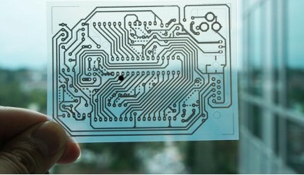
Caption main image: This single-sided wiring pattern for an Arduino microcontroller was printed on a transparent sheet of coated PET film, (Photo courtesy of Georgia Technical Institute)
Over the past decade, major advances in additive printing technologies in the 2-D and 3-D electronics fabrication space have accelerated additive processing—printing in particular—into the mainstream for the fabrication of low-cost, conformal, and environmentally friendly electronic components and systems. Printed electronics technology is opening an entirely new world of simple and rapid fabrication to hobbyists, research labs, and even commercial electronics manufacturers.
This essay originally appeared on the Circuit Cellar magazine website.
Historically, PCBs and ICs have been fabricated using subtractive processing techniques such as photolithography and mechanical milling. These traditional techniques are costly and time-consuming. They produce large amounts of material and chemical waste and they are also difficult to perform on a small scale for rapid prototyping and experimentation.
To overcome the limitations of subtractive fabrication, over the past decade the ATHENA group at the Georgia Institute of Technology (Georgia Tech) has been developing an innovative inkjet-printing platform that can print complex, vertical ICs directly from a desktop inkjet printer.
To convert a standard desktop inkjet printer into an electronics fabrication platform, custom electronic inks developed by Georgia Tech replace the standard photo inks that are ejected out of the printer’s piezoelectric nozzles. Inks for depositing conductors, insulators/dielectrics, and sensors have all been developed. These inks can print not only single-layer flexible PCBs, but they can also print complex, vertically integrated electronic structures (e.g., multilayer wiring with interlayer vias, parallel-plate capacitors, batteries, and sensing topologies to sense gas, temperature, humidity, and touch).
To create highly efficient electronic inks, which are the key to the printing platform, Georgia Tech researchers exploit the nanoscale properties of electronic materials. Highly conductive metals (e.g., gold, silver, and copper) have very high melting temperatures of approximately 1,000°C when the materials are in their bulk or large-scale form. However, when these metals are decreased to nanometer-sized particles, their melting temperature dramatically decreases to below 100°C. These nanoscale particles can then be dispersed within a solvent (e.g., water or alcohol) and printed through an inkjet nozzle, which is large enough to pass the nanoparticles. After printing, the metal layer printed with nanoparticles is heated at a low temperature, which melts the particles back into a highly conductive metal to produce very low-resistance electrical structures.
Utilizing nanomaterials has enabled the creation of plastic, ceramic, piezoelectric, and carbon nanotube and graphene inks, which are the fundamental building blocks of a fully printed electronics platform. The inks are then tuned to have the correct viscosity and surface tension for a typical desktop inkjet printer.
By loading these nanomaterial-based conductive, dielectric, and sensing inks into the different-colored cartridges of a desktop inkjet printer, 3-D electronics topologies such as metal-insulator-metal (MIM) capacitors can then be created by printing the different inks on top of each other in a layer-by-layer deposition. Since printing is a non-contact additive deposition method, and the processing temperatures are below 100°C, these inks can be printed onto virtually any substrate, including standard photo paper, plastic, fabrics, and even silicon wafers to interface with standard ICs with printed feature sizes below 20 µm.
The Georgia Tech-developed printing platform is a major breakthrough. It makes the cost of additively fabricating circuits nearly the same as printing a photo on a home desktop inkjet printer—and with the same level of simplicity and accessibility.
These advancements in 2-D electronics printing combined with current research in low-cost 3-D printing are enabling commercial-grade fabrication of devices that typically required clean room environments and expensive manufacturing equipment. Such technology, when made accessible to the masses, has the potential to completely change the way we think about building, interacting with, and even purchasing electronics that can be digitally transmitted and printed. While the printing technology is currently at a mature stage, we have only scratched the surface of potential applications that can benefit from printing low-cost, flexible electronic devices.
Benjamin Cook, who wrote this essay appearing in Circuit Cellar’s February 2014 issue, is a PhD candidate in the School of Electrical and Computer Engineering at the Georgia Institute of Technology. Circuit Cellar’s February 2014 issue will be available for download in mid-to-late January. Click here to download recent issues of the magazine.
Caption main image: This single-sided wiring pattern for an Arduino microcontroller was printed on a transparent sheet of coated PET film, (Photo courtesy of Georgia Technical Institute)
Read full article
Hide full article
Discussion (0 comments)