

Elektor Lora Node
A versatile PCB combining an STM32, an RFM95 LoRa Module and rechargeable batteries and that fits in a standard enclosure.
Elektor LoRa Node
The Elektor LoRa Node is based on the idea to have a small PCB with recharable and changable batteries, a common microcontroller, a STM32 in LQFP48, and a RFM95 LoRa Module. All this component should go into an enclosure that can be sourced at one of the bigger distributors. As the enclosure also will bound the space we can use for the energy source we need to discuss this in the first place. The first set of ideas had been to power the device from non-rechargeable batteries, but was at the same moment thrown away, as we don't want to produce any more waste of batteries, a rechargeable solution it should it be, and also easy to replace by the user. This would make a small, servable, water-resistant node, that can not only be operated under lab conditions but also take into the wild and get some real environmental data.But what is on the PCB, how long will it run, and what kind of sensors and already on board. We had a few applications in mine as we designed the first boards, but it is not bound to those. This shall be a flexible and useful platform to play with LoRa, and not even on your desk, but also to put it somewhere outside for data collection and processing. The challenge from here is the squaring of the circle, in terms of flexibility , power usage and size.
PCB design and software
From the template we generated a new board for the STM32F072 in LQFP48 , now you can use this MCU also with the Arduino IDE. This makes development pretty easy as you can now use most of your well known arduino librarys. As we don't have any kind of crystal on board we are using the internal ones. This will default here to 8MHz for the MCU to reduce the power consumption, but can be expanded up to 48MHz if desired.
You can grab the latest files form our GitHub page.
The modular approach
To meet certain points, decision were made to think in a modular way. If all components are placed, you will get LoRaWAN device with GPS module, crypto co-processor , SPI F-RAM or Flash storage. As all of this features are nice to have, not everyone will need them. Also this means, components that are not populated will save money in the basic version, and you don't need to buy features you'll never need. As the pinout for the SPI F-RAM and SPI Flash modules is standardized, you can add the module you like or you have already software around. Also for the crypto co-processor, the ATECC608a, you can also choose to just add an I²C-EEROM or F-RAM chip, meaning you have a very flexible and user configurable device at your hands. On theThis also brings us to the MCU. In the current phase we have a STM32F072 in LQFP48 on the PCB, a Cortex-M0 based one with 64kB of flash and 16k of RAM, allowing you to even have USB for firmware updates or used in your own applications.
The nice thing about the STM32 series is the pin combability. This means you can change the MCU without changing the board, e.g. you could use an even lower power STM32L072, or if you need more computation power and flash, and STM32L151. Also the STM32F103 you commonly find on the bluepill board will be can be fitted to the PCB.
So in a short summary we have the following features:
- Li-Ion powered
- User changeable cells
- STM32F072 MCU
- SPI F-RAM or FLASH (optional)
- Crypto Co-Processor (optional)
- GPS Module (optional)
- USB-Interface (optional)
PCB design and challenges
The first prototypes have been build, but we still need some adjustments. For the GPS module we need some tweaks to get better reception. You can build a miniaturized antenna but you need also take care for the ground plane. From the modules datasheet it states we need a minimum size for the PCB to have the antenna work. Currently we are not satisfied with the performance for signal reception.After the Version 1 of the board we dittched the Quectel L96 module and replaced it with the GPS Module from the Elektor Shop as this is cheaper and easyer to attatch to the board itself. Also this lead to some redesigns for the used connectors, so everything is now in a 2,54mm raster, so you can plug the module to a breadbaord of choise.
Secondly we have the RFM95 LoRa module that needs an antenna too. With the size and enclosure we choose we will use a helix one for 868MHz you can build yourself. If you like to have even better reception, an external antenna is a option. We know the design here is a compromises of space and functions and transmit and receive with the internal antenna could be better or even more optimized.
Also we have the power supply. As mentioned in the beginning we use li-Ion batteries in 10440 ( AAA ) format, you can find in e-cigarettes. These can be easy replaces by the user and charged outside the device with a proper li-ion charger. To protect the cells from deep discharge a voltage monitor ic is included that switches of the used LDO for the 3.3V supply.
Also added is now in the pinout a 2mm pinhole part to attach lopo-battery paks you normaly use for drones. This small and flat cells comes with a Molex 510005 or JST connector and offer a good capacity and space ratio. This makes the whole design more fexable and allows to use off the shelf recharable batterys that can sourced from big waarehouses starting with an A... .
The reverse current protection is now done with a loadswitch. We use the TI TPS22917 for this porpose, as it will disconnect if a certain amout of current flows reverse through the switch. Also we added a second one for the power supply towars the GPS module, so the MCU can cut power to the module to extend battery life. This also means if you don't use the GPS module in the first place you have MCU controlled switchable 3.3V you can use to power or disable other external circutry.
Powering the device form NiMH-Cells would be possible but needs additional circuits, in this case a DC/DC boost stage. As the boost stage will consume power all the time this may reduce runtime, and we also need to reconsider the under voltage lockout.
Suggestions are welcome
As we are still in the prototype we would love to have your suggestions and ideas for the project. As this is an experimental platform for LoRa fell free to add your ideas, concerns and features so we can improve the project. The main points we need to improve currently is GPS reception, LoRa Antenna and the some tweaks in the power supply.
[Update 24.10.2019 ]
Hardwareside
Version 3.0 has arrived in the Lab and almost all parts, only the TPS22917 load switches are currently missing. We have done the first Test on the PCB and so far all assambled hareware seem to work as intended. The STM32 runs at 8MHz and can communicate with the LoRa Module on the board. Also our selfmade antenna is transmitting fine.
The biggest challanges are now within the software. As test setup we are doing point to point communication in the RAW mode that is offered by the LMIC library. Also the batterys have charged and all cables are attached. Currently the next thing is to get the software parts for the upcomming projects in place.
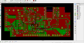
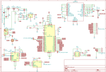
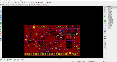
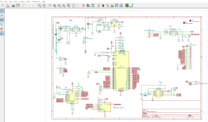
The good news about the project for you is that all files for the hardware will be released under Creativ Commons 4.0 Share Alike ( CC-BY-SA ), mening you can grab your copy of KiCad and have a look yourself. Yurrently we need to prepere some files. But to avoid just boring text here some screeshots from the current development.
The rest of the board is working as expected, no fancy magic included. If you ask if this is final, well, there is one stupid choise of pins done. It was originally planned to have a secondary SPI port on the connector, sadly on pin that is reqiered is currently use to monitor the battery voltage at the input. Lesson learned, read the data sheet twice. If there will be a Revision 3.1, we will see as this needs to be discussed if it is ready in time. Also we need to do some testruns with the TPS22917 to verfiy if the chip works as intended. If so, or if not , we will update this post and let you know what happend.
Softwareside
Now to the software part. As the software nower days defines more and more the fnctions and use for hardware, it is still for some just a kind of black magic that needs to be flashed. If you compare in this projetc the time spend on software and hardware, software took most of the time. So where was and is the time spend. As mentioned in the beginning you can programm the baord with your arduino ide of choise. For this the stm32duino project has done great work to support a wide range of STM32 mcus, in general all STM32 families are supported. A bunch of baords are supported, and for those who like to add support for their own baords a template is porvided to add those.Adding the LoRA Node Experimental Platform was the first task that needed to be done. In the arduino core for the stm32 we neede to edit a few files and add the board definition, to be ready to go. After some errors and unexpected software behaviour we got the template running and could start coding the first few lines.
On thing you normally don't care about is the way the mcu gernerates the clock. On the older AVR chips you had a crystal and thats it. On the more recent mcus you have more options to gernate the mcu main clock, often from internal PLL / FLL sources or high speed internal RC oscillators. We choose to use the internal clock sources, as those are not really great for freqnecy stability, but good enough to get us going. Also we are able to change the clockspeed during runtime so we can run at low rates if we need to safe power or get to higer ones if we need more processing power. As a default we have choosen 8Mhz for the core and peripherals, as this will reduce power consumption and is fast enoigh to process the LoRa stack.
The challanges ahead is to potimize power consumption and also to initilaize all componets in a usable way. As this is project specific, have a look at the LoRa Switch with state feedback, as this shows how to use the LoRa Stack in RAW mode to do some peer to peer communication.
[Update 31.10.2019]
We have now PCB V3.1 ready. Changes were done mainly to get the compleate secondary SPI to the spare pins and also to optimize some parts in the power input. The TI Loadswitch has been exchanged by a pin compatible "ideal" diode which will give us reverse current protection and will also enable the Board to run form two power supplys with one serving as backup.
As we don't have a crystal as main clock surce but depend on the internal ones we added a 32.768kHz oscillator for the RTC domain. This one can be placed optionally and has be used in the DS1302 High precision RTC . Wih a few uA of current we gain UARTs that can be clock from the crystal and also we gain a RTC that can wake the MCU after a given timeframe from sleep.
Last but not least, we squeezed two leds ( one red and one green ) on the board to give the chance to signel some kind of status. For this we used PA15 and PB3. These Pins are also on the pinheader as JTDO and JTDI.
If nothing really bad happens we should be good to go. The PCBs have been orderd and shall arrive next week. As Version 3.0 of the PCB is now running as expected we don't expect heavy problems with the new one, but we keep the fingers crossed, as always somthing unexpected can happen. Also we start preparing the final files for GitHub in the next few days as some cleanup has to be done.
[Update 8.11.2019]
PCB in Version 3.1 has arrived and two of them have been assembeld and are working. Some minor glitches do remain as the schematic now indecates that the tlv809 is moved closer to the battery input and between this and the idela diode is a polyfuse placed. As this seems a not that bad idea, the pcb will draw a hig current when first connected to the battery. The first research showed that this is not due to the 470uF capacitor as main source but seems to be something with the EN input of the MAX40200 ideal diode.
The assumption is that EN will be at a higher voltage level on power up than the ideal diode and therfore a unexpected high current will fow through a part we still need to determin. Switching from an TLV809 with push-pull to a TLC803S with open drain output should resolve the problem, but the lab needs some moments to verify that this is the main issue.
[27.11.2019]
Current PCBs seems to work fine with the TLV809 / MAX809 if used with a LiPo-Cell, also works fine is powered from 5V USB.
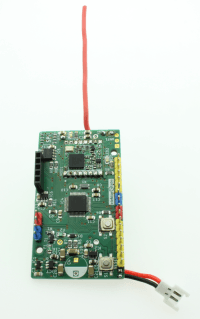
So it's time for final pcitures and some renderings.
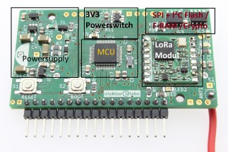
As you can see the the Board and its functions are build in sections. Left you can see the powersupply handlelung the undervoltage lockout and 3.3V to the MCU. In the middle top you can see a 3.3V switch for peripherals you'll need for powersavings to cut VCC. On the left you will find the two SO-8 sockets for an SPI Flash or FRAM and an I²C-Socket for EEPROMS / FRAM or Crypto-Co-Porcessors. Usually you don't need them to be populated so we leave it to you if you like to use them or not
As antenna you can use a peace of 8,2cm long wire for 868MHz, or any other commercial antenna that is for the 868MHz band usable. When it comes to firmware development for the board you can choos the bare metal C-Way with the STMCubeIDE or the Arduino IDE to programm the Node with ease. To do so you need to download the Arduino IDE and the STM32 Arduino Core. In the Arduino IDE add to the Additional Boards Manager URL : https://github.com/stm32duino/BoardManagerFiles/raw/master/STM32/package_stm_index.json and install the STM32 Boards following the instructions at https://github.com/stm32duino/wiki/wiki/Getting-Started .
A this point you got the STM32 core but for the Elektor LoRa Node you need to add a few things to you local filesystem. For Windows go to " %localappdata%\Arduino15\packages\STM32\hardware\stm32\1.7.0 %localappdata%\Arduino15\packages\STM32\hardware\stm32\1.7.0 " and add at the end of the Boards.txt the content of the here attached zip file included „Add_To_Board.txt“ . Also copy the ELEKTOR_LORA_NODE_CORE_F072xC folder to the variants folder. Now you should be good to go and compile software for the board. At the end you need to set the follwing Boardsettings:

At this point you are good to go to compile software for the baord. To do an upload you need to install the STM32CubeProgrammer from https://www.st.com/en/development-tools/stm32cubeprog.html . If you now like to upload code put the board into bootloder mode by pressing boot and short toggeling the reset button. Now you can upload new Firmware to the board.
[ Update 3.12.2019]
The board definitions have been merged into the official STM32Arduino git repository. So the next release you no longer need to patch something and can easy select the board form the Arduino Boards menu.
[ Update 17.03.2020 ]

The board is now included in the STM32duino and also some minor tweeks have been done to get everything working. This means that you can also use goodies like a second UART or the low power one for wakeup in UART data. This way you can use your arduino librarys as with other boards. Also the sleep mode is working and currently we can get down to 140µA while the MCU sleeps and the content in RAM is keept. With a set of lithum batteries this gives you a decent time to sleep and wait fot something to happen. But be warned, even if 64kB of flash seem a lot, and still are, with code form the arduino world this gets really fast filled up.
Discussion (2 comments)
schofiel 3 years ago
This would be the LoRa Button (180666-2) and the LoRa AC Switch (180666-2).
ElektorLabs 3 years ago
schofiel 4 years ago
https://github.com/ElektorLabs/180516-Elektor_LoRa_Node