
Voltage-level shifter for 3-state output
I’ve seen some Arduino users needing extra RAM, and looking at the SPI-connected 23K256 SRAM chip. The trouble is that the 23K256 has a maximum operating voltage of 3.6V, while the Arduino uses a 5V power supply.
I’ve seen some Arduino users needing extra RAM, and looking at the SPI-connected 23K256 SRAM chip. The trouble is that the 23K256 has a maximum operating voltage of 3.6V, while the Arduino uses a 5V power supply.
On the Internet, one can easily find bad solutions. Some even suggest to run the 23K256 at 5V, above its absolute maximum rating. So I wanted to find a better way to connect a 23K256 chip to an Arduino board.
Fortunately, Arduino boards have a 3.3V regulated output that can be used to power the 23K256 chip. It is also quite easy to adapt the SS, SCLK and MOSI signals with simple 2-resistor voltage dividers, as they are 2-state Arduino -> 23K256 signals.
As for the MISO signal, it is a little more complex. A N-channel MOSFET used in a common-gate configuration, with two pull-up resistors, is commonly used for I²C signals. But then the H and Z states are mixed in a single middle-Z high-level state. Parasitic capacitors will make the rise time long. One could also use a TXB0104 bidirectional voltage-level shifter. Somewhat better, but still no real Z state. Moreover, the impedance of the output is low for a short time, and then gets higher to allow bidirectional use. Last but not least, I guess many electronics enthousiasts don’t have those in stock.
So I began to think about a better solution to shift the voltage-level of a 3-state output, with very common components. I found out the solution below, with 4 BJT and 6 resistors. Built on a solderless breadboard, it works fine with signals up to 1MHz. I will make a PCB for this to find out how it performs without the parasitic capacitors of a solderless breadboard.
Update 1: adding a pair of shottky prevent the output transistors for saturating, which significantly improve the response time. Now, signals up to 3MHz are handled properly, still on a solderless breadboard. Next step: make a PCB and test how it performs.
Update 2: something was plain wrong with this circuit. When SO is low, Q1’s Vce is close to 0, so this transistor has very bad performace (low gain and high turn-off time). A pair of resistors between the SO input and Q1 and Q2 bases improves things significanty. Moreover, a pair of capacitors connected in parallel to the new resistors compensate the parasitic capacitors (of the transistors and of the circuit). On my prototype, on a solderless breadboard, 22pF capacitors gave good results.
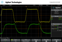
Update 3: I finally built the circuit on a PCB and tested it with a 4MHz square signal in input. The output is qute clean , with a delay lower than 30ns, somewhat better than I expected.
May I still improve it with very common components?
Want to build a project?
Bring your design to life with the Elektor PCB Service, powered by Eurocircuits. Upload the project files and order professionally manufactured PCBs or assembled boards through a proven European production platform.
Supporting KiCad, Eagle, Gerber, and ODB++ formats, the service is suitable for everything from prototypes and validation builds to series production and volume manufacturing.
Made in Europe. Fast. Reliable. Professional.
Discussion (1 comment)