

Record: lowest embedded SRAM power
June 13, 2017
on
on
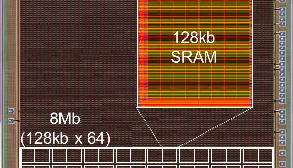
13.7 nW/Mbit is claimed by Renesas as a record low stand-by power for embedded SRAM. Speed has been retained at 1.8 ns for an active read-out. The firm said it used its in-house 65-nm silicon-on-thin buried oxide (SOTB) process for the prototype, and used substrate biasing to adjust the leakage/speed compromise. The technology is claimed overcome challenges with conventional CMOS, such as the increased leakage with low-threshold transistors and high variability in gate threshold voltage.
A major source of threshold variation in conventional small transistors is that there are so few dopant atoms in the channel that a handful either way changes the threshold. With STOB, and other fully-depleted silicon-on-insulator (FDSoI) processes, reportedly there are no dopant atoms in the transistor channel to vary in number.
Normal to high-speed mode (zero substrate bias to forward bias) changes read access time of the new devices from 4.58 to 1.84 ns.
Reverse-bias in stand-by mode cuts leakage is a factor 1,000 down compared with normal mode –- to the record-setting 13.7 nW/Mbit figure.
The research work leading up to the prototype was presented at the VLSI Symposia in Kyoto on June 8. Renesas expects to use the technology as an alternative to non-volatile memory for energy-harvesting and battery-powered applications in IoT, home electronics, and healthcare.
Read full article
Hide full article
Discussion (0 comments)