
Three Baristor circuits for experimentation
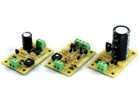
Two Baristor circuits from the book ‘Electronic Circuits For All’ plus one from the lab to experiment with and maybe solutions for other project ideas
160512-1
This a circuit taken from the book ‘Electronic Circuits For All’ by M.A. Shustov and A.M. Shustov (https://www.elektor.com/electronic-circuits-for-all). We selected a few of them and designed PCBs to make testing and experimenting easier. Many circuits are small enough to be tested on a breadboard. This is a circuit that uses a baristor to make a simple power supply, specifically based on a switching single-threshold baristor with controlled threshold value. As the authors define a baristor; “The barrier-resistor element (barrier + resistor = baristor) is a switch element of power and analogue electronics, whose electrical “Input-Output” resistance changes abruptly from a conducting state to a non-conducting state or vice versa. Thereby the change condition is fulfilled when the predetermined threshold value (barrier) of the input signal is reached”.
This circuit is a practical scheme of a power supply based on switching single-threshold baristors with controlled threshold value. The circuit from the book shows 47 Ω for R1 and R2 and 200 kΩ for R3. But this can never work. T1 and T2 will never conduct. About 0.56 V across R1 and R2 would be needed and 12 mA would have flow through R1 and R2 which will never happen. The circuit was already published in 2004 in ‘Практическая схемотехника Полупроводниковые приборы и их применение Книга 5’ (Practical Circuitry Semiconductor Devices and their application Book 5) by M.A. Shustov using Russian made transistors KT315 (NPN), KT361 (PNP) and KT805AM (NPN power). In that version R1 and R2 show a value of 680 Ω and 5.1 kΩ is used for R3 and are more realistic. But values also depend on the transistors used. 470 kΩ or 330 kΩ for P1 is too high, even a 100 kΩ trimmer only has a small part where the output voltage changes and so the value of P1 may even be lower. This circuit can certainly be improved on, meaning not just changing component values but the entire circuitry. For instance something like this perhaps (not tested by us):
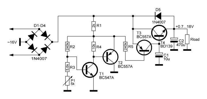
About our circuit (160512-1). A power supply with a baristor contains a rectified AC voltage (about 16 VAC is used in this case) a threshold and key elements. If the voltage at the output of the bridge rectifier D1..D4 doesn’t exceed the threshold set by T1/T2 than composite transistor T3/T4 is conducting. The actual voltage level from D1..D4 minus the voltage drop across T4 is stored in buffer capacitor C1. If the input voltage exceeds the threshold T4 is blocking and the output voltage is not increasing any further. This way, depending on the threshold level set by T1 and T2, the output voltage can be set by P1. Replacing P1 by an optocoupler or a JFET the output voltage can be controlled by another circuit. If the applied AC voltage is higher resistors R3 and R4 should be changed accordingly. Depending on the values of the resistors and other conditions, the current-voltage characteristic of the circuit around T1/T2 varies from "thyristor" to "Zener diode". The problem with this is it’s not really a zenerdiode. If T1 and T2 are not conducting there is still current flowing through R2-P1-R1-R3. So if P1 is to low or R3 to high T3 may switch on or off and there’s no real threshold and the output voltage varies with the AC input voltage. Also some very low frequency instability can occur at certain settings of P1 in combination with different AC input voltages. Also the output impedance of the transformer influences the operation and stability of the circuit.. A 10 µF capacitor from base of T4 to ground can approve circuit stability. A change in load resistance will change the output voltage.
Some measurements (150 Ω load and a specific setting of P1):
AC in DC out
12 V 11.4 V
16 V 9.9 V
20 V 9 V
24 V 8.6 V
At 20 VAC input voltage the output voltage drops from 9 to 6.7 V when the load resistance is halved to 75 Ω
At certain input voltages and settings of P1 the output voltage fluctuates over time.
No load current can be less than 1 mA but also several mA’s, depending on the setting of P1, input voltage and load removal.
Bill of materials 160512-1 v1.1
Resistor
R1,R2 = 680 Ω, 5%, 0.25W
R3 = 5.1 kΩ, 1 %, 0.25W
R4 = 220 kΩ, 5 %, 0.25 W
P1 = 100 kohm, 20 %, 0.15 W, trimmer (CB10LV104M Citec-TE Connectivity)
Capacitor
C1 = 470 µF, 20 %, 50 V, diam. 13 mm, pitch 5 mm
Semiconductor
D1,D2,D3,D4,D5 = 1N4007
T1,T3 = BC557B
T2 = BC547B
T4 = BD139
Other
K1,K2 = 2ways PCB Terminal Block, 5.08 mm (MKDSN 1,5/ 2-5,08 Phoenix Contact)
Misc.
PCB 160512-1 v1.1
160512-2
PCB 160512-2 v2.0 modified to v2.1 (4 x 47 nF parallel to D1..D4)
This circuit taken from the book ‘Electronic Circuits for All’ by M.A.. Shustov and A.M. Shustov is slightly improved. Its purpose isn’t so much a full working device but a circuit that can be modified to fit your own applications or just give new ideas or be part of a solution for other purposes. The PCB makes testing and experimenting easier but the circuit is simple enough to be tested on a breadboard.
A positive feedback (R7, C5) is added to suppress erroneous switching and to enhance switching of the output stages. This makes the base of T1 act like the input of a Schmitt-trigger. Due to the hysteresis, which depends on the applied AC voltage to K1, the phase set with P1 changes with the level of the input voltage. Depending on the application and AC voltage used the values of some components probably have to be modified. Helpful can be the use of simulation software like LTSpice. Using a voltage source instead of a “real” transformer in the simulation will give false results. Every transformer has a complex output impedance consisting mainly of a combination of a resistance and an inductance. This means the moment the Baristor switches the input voltage changes and can cause instability, especially when the gain of T1 is very high.
The original circuit used High Voltage Darlington’s of type BC373, these are hard to find. The specifications are 80 V / 1 A in a TO92 case style. hFE at 100 mA is more than 20000. Fortunately there are quite a few replacements. Here is a small list of types that are still available:
BCX38C, 60 V / 0.8 A
KSP13B, 30 V / 0.5 A
MPSA14, 30 V / 0.5 A
MPSA29, 100 V / 0.5 A
ZTX603, 80 V / 1 A
ZTX605, 120 V / 1 A
ZTX614, 100 V / 0.8 A
BC517-D74Z, 30 V / 1.2 A (collector and emitter connections swapped!)
But be careful using a TO92 as an output transistor, due to the limited maximum power dissipation of this package it’s wise to use a larger case style. We used the good old BD139 in combination with a standard BC547C to make a discrete Darlington replacement for the originally used BC373. The BD139 has a SOT32 (TO126) case style and allows a maximum power dissipation of 1.25 W without additional cooling (junction will be 150 °C at a room temperature of 25 °C). Never use a transistor at a junction temperature of 150 °C, keep it below 70 °C if you don’t want to reduce its lifespan. And why not use a BD679 Darlington the reduce the number of parts you might ask? Well almost all Power Darlington’s have resistor build in resistors, parallel to the base-emitter of both transistors. These cause the gain of the transistor to vary with the collector current. And at low currents the gain is much lower than compared to Darlington’s without these build-in resistors.
Measurements
Maximum voltage drop from K1 to K2/K3 is about 4 V at 100 mA due to D1…D4 and a small voltage drop across R4 and R6 and the base-emitter voltages of T2/T3 and T5/T6. So without extra cooling of T3/T6 the maximum output current should be limited to a few 100 mA.
Our test setup uses a variable autotransformer, maybe better known under the trademark name Variac. It’s used to vary the primary voltage of safety transformer type FL 30 / 12 from Block. It has two primary windings of 115 V and two secondary windings of 12 V able to supply 1.25 A each. This way a safe test setup is guaranteed. But be very careful in this setup. The maximum output voltage of the autotransformer is typically higher than the input voltage. I used one that is still specified for use with 220 V mains voltage. The output is specified as 250 V / 2 A. At the present mains voltage of 230 V at my location the no load output voltage is even higher, 261 V. But it’s even worse when measuring the output voltage it was 274V, the mains voltage was 239 V at that time. In any case, never adjust the autotransformer to its maximum voltage in this test setup. This will most certainly destroy the safety transformer connected to it.
In a first test a small transformer was used and R7/C5 were enough to get rid of the erroneous switching. But using the test setup as described above this wasn’t enough. The four diodes of the rectifier had to be decoupled with 4 x 47 nF.
Removing D5 will increase the range of P1 and has more effect at low input voltages. To change the range of P1 at high input voltages consider changing R1 and R3 also, and maybe the working voltage of D5. But due to the low current flowing through D5 the voltage drop across it is less than the rated working voltage.
An example of maximum phase angles at minimum and maximum setting of P1 (18 V at K1):
P1 full clockwise: 29° - 148°
P2 full anti clockwise: 79° - 126°
No load current: 1.71 mA (12 V at K1)
No load current: 3.75 mA (24 V at K1)
Load impedance at K2 is the same as at K3:
Input current: (Uin – 3.2 V)/Rload, measured at 300 mA (K1) and 75 Ω loads
Input current : (Uin – 3 V)/Rload, measured at 120 mA (K1) and 75 Ω loads
With two identical loads connected to K2 and K3 the input current is virtually independent of the setting of P1 and varies only slightly, a few percent., due to component tolerances.
Bill of material PCB 160512-2 v2.1
Resistor
R1 = 56 kΩ, 5%, 0.25W
R2 = 1 MΩ, 5%, 0.25W
R3 = 180 kΩ, 5%, 0.25W
R4,R6 = 6.8 kΩ, 5%, 0.25W
R5 = 330 kΩ, 5%, 0.25W
R7 = 1.5 MΩ, 5%, 0.25W, 250V
P1 = Trimmer Potentiometer, 100 kohm
Capacitor
C1,C2,C3,C4 = 47 nF, 50 V, ceramic X7R, 2.54 mm pitch
C5 = 1 nF, 100 V, ceramic X7R, 2.54 mm pitch
Semiconductor
D1,D2,D3,D4 = 1N4007
D5 = BZX79-C3V0, 3 V, 500 mW
T1,T4 = BCX38C, darlington, 60 V, 0.8 A
T2,T5 = BC547C
T3,T6 = BD139
Other
K1,K2,K3 = 2ways PCB Terminal Block, 5.08 mm, MKDSN 1,5/ 2-5,08
Misc.
PCB 160512-2 v2.1
160512-3
To give an idea what else is possible we designed a little circuit with a Baristor functionality (160512-3) that produces a DC output voltage less dependent on load and AC input voltage using a minimum of parts. The principle is simple. The output stage acts as a switch and needs to be turned off as soon as the input voltage rises above a certain threshold. That threshold is mainly set by Zener diode D5. R1 limits the current at higher input voltages and R2 makes sure some current flows through the Zener before discrete Darlington T1/T2 turns on. T1/T2 pull the base of composite transistor T3/T4 to ground, thereby turning off the output switch. To make the dropout voltage across T4 minimal we used a combination of an NPN small signal and a PNP power transistor, this saves a few tenths of volts. To make the drop due to the base current through R3 even lower the value of R3 is just 1 kΩ. This latter means a quarter watt resistor will dissipate its maximum power at 21 V input voltage. So the following measurements with input voltages above 21 V make R3 exceed its specifications. In that case use a type of resistor with a similar package but with 0,5 or 0,6 watt specification. There are also types with a 1 Watt specification in this package. Mount such a resistor slightly above the PCB. Dissipation will be largest with no load. Since the T3/T4 will be turned off permanently the voltage across R3 is almost all input voltage, minus voltage drop across the bridge rectifier. The fact that T1/T2 turn on above a certain voltage doesn’t change much. With a Zener of 4.7 V (0.5 W) the output voltage is approximately 4,4 V with a 150 Ω load. A 10 Ω load reduces the output voltage to a little less than 4 V. No load voltage is about 4.67 V. Originally we used a good old BD140. At low output current it works well. But with a higher load, such as 10 Ω resistor, it almost immediately short circuited. Our test setup is able to deliver a nominal 1.25 A AC RMS current, so peak even more. A BD140 can handle 1.5 A peak currents which especially with a large capacitor at the output is not enough. I replaced it with a BD440 from an old stock but this type is still available (BD440S, Mouser 512-BD440S). The BD440 is a 60 V/ 4 A (7 A pulse) PNP power transistor. There are other suitable candidates in a TO-126 (SOT-32) package to replace T4 like a 2N5195 (PNP, 80 V, 4 A), BD438 (45 V, 4 A) or BD442G (80 V, 4 A). Depending on the manufacturer lead spacing can differ somewhat, instead of 2.29 mm 2.39 mm (TO−225AA). Also the transistor package can be a little bigger like 14.2 x 8 mm instead of the original TO-126 dimensions of 11.1 x 7.8 mm. But all of these should still fit on the PCB. The footprint for large buffer capacitor C1 is designed for capacitors with a lead spacing of 5, 7,5 and 10 mm and a maximum can diameter of 22 mm (no snap-in pins just straight leads).
Michel Shustov had a look at this circuit and suggested a modification to make the output adjustable by replacing R2 by a potentiometer. The output is indeed adjustable this way but at higher voltages the output voltage becomes more and more dependent on the input voltage. The voltage across R1 will increase more with a lower value of P1and becomes more and more dominant than the Zener voltage. To set a different output voltage it’s best to change the Zener voltage. If surges at the bridge rectifier occur these can be reduced by placing a diode between D5 and R3.
Although all three circuits are working but they are experimental and not to be considered really finished projects, lack current and/or overload protection for instance. Also temperature of the output power transistors should be monitored at higher loads and input voltages. Consider attaching a small aluminum plate or something similar to the power transistor(s) for cooling.
A few measurements (160512-3 v1.0, T4 = BD440):
150 Ω load:
Uin[V] In[mA] Uout[V]Uripple[mV]
AC AC DC ACpp
5 44 4.28 24
6 64 4.48 56
7 74 4.46 60
8 80 4.44 60
9 85 4.43 60
10 89 4.42 60
11 92 4.42 60
12 94 4.41 60
13 96 4.41 60
14 98 4.40 60
15 101 4.39 60
16 102 4.38 60
17 104 4.37 60
18 106 4.36 60
19 109 4.36 60
20 110 4.35 60
21 110 4.34 60
22 111 4.33 60
23 112 4.33 60
24 113 4.32 60
At low loads most input current is caused by pulling R3 to ground by T1/T2. For use with very low loads consider increasing the value of R3. Drop across T4 may increase but it may increase overall efficiency. Something to experiment with.
A mall test with a much higher load of 10 Ω was also performed. At 12 V input voltage the input current for a 10 Ω load is 0.57 A. The output voltage is 3.99 V. But T4 gets hot without cooling! Efficiency is not great but is more complex than multiplying voltages and currents since currents and voltage in a Baristor are anything but sinusoidal. Compare this to triac and thyristor circuits. The use of a Baristor causes a lot of harmonics and for any end user the addition of a good filter is mandatory.
Bill of materials PCB 160512-3 v1.0
Resistor
R1,R2 = 10 kΩ, 5%, 0.25W
R3 = 1 kΩ, 5%, 0.25W
Capacitor
C1 = 4700 µF, 50 V, 20 %, diam. 22 mm max, lead spacing 5/7.5/10 mm
Semiconductor
D1,D2,D3,D4,D6 = 1N4007
D5 = BZX55C4V7, 4.7 V, 500 mW
T1,T2,T3 = BC547C
T4 = BD440 (PNP, 60 V, 4 A, 7 A pulse, TO-126)
Other
K1,K2 = Terminal block 5.08 mm, 2-way, 630 V
Misc.
PCB 160512-3 v1.0
This a circuit taken from the book ‘Electronic Circuits For All’ by M.A. Shustov and A.M. Shustov (https://www.elektor.com/electronic-circuits-for-all). We selected a few of them and designed PCBs to make testing and experimenting easier. Many circuits are small enough to be tested on a breadboard. This is a circuit that uses a baristor to make a simple power supply, specifically based on a switching single-threshold baristor with controlled threshold value. As the authors define a baristor; “The barrier-resistor element (barrier + resistor = baristor) is a switch element of power and analogue electronics, whose electrical “Input-Output” resistance changes abruptly from a conducting state to a non-conducting state or vice versa. Thereby the change condition is fulfilled when the predetermined threshold value (barrier) of the input signal is reached”.
This circuit is a practical scheme of a power supply based on switching single-threshold baristors with controlled threshold value. The circuit from the book shows 47 Ω for R1 and R2 and 200 kΩ for R3. But this can never work. T1 and T2 will never conduct. About 0.56 V across R1 and R2 would be needed and 12 mA would have flow through R1 and R2 which will never happen. The circuit was already published in 2004 in ‘Практическая схемотехника Полупроводниковые приборы и их применение Книга 5’ (Practical Circuitry Semiconductor Devices and their application Book 5) by M.A. Shustov using Russian made transistors KT315 (NPN), KT361 (PNP) and KT805AM (NPN power). In that version R1 and R2 show a value of 680 Ω and 5.1 kΩ is used for R3 and are more realistic. But values also depend on the transistors used. 470 kΩ or 330 kΩ for P1 is too high, even a 100 kΩ trimmer only has a small part where the output voltage changes and so the value of P1 may even be lower. This circuit can certainly be improved on, meaning not just changing component values but the entire circuitry. For instance something like this perhaps (not tested by us):
About our circuit (160512-1). A power supply with a baristor contains a rectified AC voltage (about 16 VAC is used in this case) a threshold and key elements. If the voltage at the output of the bridge rectifier D1..D4 doesn’t exceed the threshold set by T1/T2 than composite transistor T3/T4 is conducting. The actual voltage level from D1..D4 minus the voltage drop across T4 is stored in buffer capacitor C1. If the input voltage exceeds the threshold T4 is blocking and the output voltage is not increasing any further. This way, depending on the threshold level set by T1 and T2, the output voltage can be set by P1. Replacing P1 by an optocoupler or a JFET the output voltage can be controlled by another circuit. If the applied AC voltage is higher resistors R3 and R4 should be changed accordingly. Depending on the values of the resistors and other conditions, the current-voltage characteristic of the circuit around T1/T2 varies from "thyristor" to "Zener diode". The problem with this is it’s not really a zenerdiode. If T1 and T2 are not conducting there is still current flowing through R2-P1-R1-R3. So if P1 is to low or R3 to high T3 may switch on or off and there’s no real threshold and the output voltage varies with the AC input voltage. Also some very low frequency instability can occur at certain settings of P1 in combination with different AC input voltages. Also the output impedance of the transformer influences the operation and stability of the circuit.. A 10 µF capacitor from base of T4 to ground can approve circuit stability. A change in load resistance will change the output voltage.
Some measurements (150 Ω load and a specific setting of P1):
AC in DC out
12 V 11.4 V
16 V 9.9 V
20 V 9 V
24 V 8.6 V
At 20 VAC input voltage the output voltage drops from 9 to 6.7 V when the load resistance is halved to 75 Ω
At certain input voltages and settings of P1 the output voltage fluctuates over time.
No load current can be less than 1 mA but also several mA’s, depending on the setting of P1, input voltage and load removal.
Bill of materials 160512-1 v1.1
Resistor
R1,R2 = 680 Ω, 5%, 0.25W
R3 = 5.1 kΩ, 1 %, 0.25W
R4 = 220 kΩ, 5 %, 0.25 W
P1 = 100 kohm, 20 %, 0.15 W, trimmer (CB10LV104M Citec-TE Connectivity)
Capacitor
C1 = 470 µF, 20 %, 50 V, diam. 13 mm, pitch 5 mm
Semiconductor
D1,D2,D3,D4,D5 = 1N4007
T1,T3 = BC557B
T2 = BC547B
T4 = BD139
Other
K1,K2 = 2ways PCB Terminal Block, 5.08 mm (MKDSN 1,5/ 2-5,08 Phoenix Contact)
Misc.
PCB 160512-1 v1.1
160512-2
PCB 160512-2 v2.0 modified to v2.1 (4 x 47 nF parallel to D1..D4)
This circuit taken from the book ‘Electronic Circuits for All’ by M.A.. Shustov and A.M. Shustov is slightly improved. Its purpose isn’t so much a full working device but a circuit that can be modified to fit your own applications or just give new ideas or be part of a solution for other purposes. The PCB makes testing and experimenting easier but the circuit is simple enough to be tested on a breadboard.
A positive feedback (R7, C5) is added to suppress erroneous switching and to enhance switching of the output stages. This makes the base of T1 act like the input of a Schmitt-trigger. Due to the hysteresis, which depends on the applied AC voltage to K1, the phase set with P1 changes with the level of the input voltage. Depending on the application and AC voltage used the values of some components probably have to be modified. Helpful can be the use of simulation software like LTSpice. Using a voltage source instead of a “real” transformer in the simulation will give false results. Every transformer has a complex output impedance consisting mainly of a combination of a resistance and an inductance. This means the moment the Baristor switches the input voltage changes and can cause instability, especially when the gain of T1 is very high.
The original circuit used High Voltage Darlington’s of type BC373, these are hard to find. The specifications are 80 V / 1 A in a TO92 case style. hFE at 100 mA is more than 20000. Fortunately there are quite a few replacements. Here is a small list of types that are still available:
BCX38C, 60 V / 0.8 A
KSP13B, 30 V / 0.5 A
MPSA14, 30 V / 0.5 A
MPSA29, 100 V / 0.5 A
ZTX603, 80 V / 1 A
ZTX605, 120 V / 1 A
ZTX614, 100 V / 0.8 A
BC517-D74Z, 30 V / 1.2 A (collector and emitter connections swapped!)
But be careful using a TO92 as an output transistor, due to the limited maximum power dissipation of this package it’s wise to use a larger case style. We used the good old BD139 in combination with a standard BC547C to make a discrete Darlington replacement for the originally used BC373. The BD139 has a SOT32 (TO126) case style and allows a maximum power dissipation of 1.25 W without additional cooling (junction will be 150 °C at a room temperature of 25 °C). Never use a transistor at a junction temperature of 150 °C, keep it below 70 °C if you don’t want to reduce its lifespan. And why not use a BD679 Darlington the reduce the number of parts you might ask? Well almost all Power Darlington’s have resistor build in resistors, parallel to the base-emitter of both transistors. These cause the gain of the transistor to vary with the collector current. And at low currents the gain is much lower than compared to Darlington’s without these build-in resistors.
Measurements
Maximum voltage drop from K1 to K2/K3 is about 4 V at 100 mA due to D1…D4 and a small voltage drop across R4 and R6 and the base-emitter voltages of T2/T3 and T5/T6. So without extra cooling of T3/T6 the maximum output current should be limited to a few 100 mA.
Our test setup uses a variable autotransformer, maybe better known under the trademark name Variac. It’s used to vary the primary voltage of safety transformer type FL 30 / 12 from Block. It has two primary windings of 115 V and two secondary windings of 12 V able to supply 1.25 A each. This way a safe test setup is guaranteed. But be very careful in this setup. The maximum output voltage of the autotransformer is typically higher than the input voltage. I used one that is still specified for use with 220 V mains voltage. The output is specified as 250 V / 2 A. At the present mains voltage of 230 V at my location the no load output voltage is even higher, 261 V. But it’s even worse when measuring the output voltage it was 274V, the mains voltage was 239 V at that time. In any case, never adjust the autotransformer to its maximum voltage in this test setup. This will most certainly destroy the safety transformer connected to it.
In a first test a small transformer was used and R7/C5 were enough to get rid of the erroneous switching. But using the test setup as described above this wasn’t enough. The four diodes of the rectifier had to be decoupled with 4 x 47 nF.
Removing D5 will increase the range of P1 and has more effect at low input voltages. To change the range of P1 at high input voltages consider changing R1 and R3 also, and maybe the working voltage of D5. But due to the low current flowing through D5 the voltage drop across it is less than the rated working voltage.
An example of maximum phase angles at minimum and maximum setting of P1 (18 V at K1):
P1 full clockwise: 29° - 148°
P2 full anti clockwise: 79° - 126°
No load current: 1.71 mA (12 V at K1)
No load current: 3.75 mA (24 V at K1)
Load impedance at K2 is the same as at K3:
Input current: (Uin – 3.2 V)/Rload, measured at 300 mA (K1) and 75 Ω loads
Input current : (Uin – 3 V)/Rload, measured at 120 mA (K1) and 75 Ω loads
With two identical loads connected to K2 and K3 the input current is virtually independent of the setting of P1 and varies only slightly, a few percent., due to component tolerances.
Bill of material PCB 160512-2 v2.1
Resistor
R1 = 56 kΩ, 5%, 0.25W
R2 = 1 MΩ, 5%, 0.25W
R3 = 180 kΩ, 5%, 0.25W
R4,R6 = 6.8 kΩ, 5%, 0.25W
R5 = 330 kΩ, 5%, 0.25W
R7 = 1.5 MΩ, 5%, 0.25W, 250V
P1 = Trimmer Potentiometer, 100 kohm
Capacitor
C1,C2,C3,C4 = 47 nF, 50 V, ceramic X7R, 2.54 mm pitch
C5 = 1 nF, 100 V, ceramic X7R, 2.54 mm pitch
Semiconductor
D1,D2,D3,D4 = 1N4007
D5 = BZX79-C3V0, 3 V, 500 mW
T1,T4 = BCX38C, darlington, 60 V, 0.8 A
T2,T5 = BC547C
T3,T6 = BD139
Other
K1,K2,K3 = 2ways PCB Terminal Block, 5.08 mm, MKDSN 1,5/ 2-5,08
Misc.
PCB 160512-2 v2.1
160512-3
To give an idea what else is possible we designed a little circuit with a Baristor functionality (160512-3) that produces a DC output voltage less dependent on load and AC input voltage using a minimum of parts. The principle is simple. The output stage acts as a switch and needs to be turned off as soon as the input voltage rises above a certain threshold. That threshold is mainly set by Zener diode D5. R1 limits the current at higher input voltages and R2 makes sure some current flows through the Zener before discrete Darlington T1/T2 turns on. T1/T2 pull the base of composite transistor T3/T4 to ground, thereby turning off the output switch. To make the dropout voltage across T4 minimal we used a combination of an NPN small signal and a PNP power transistor, this saves a few tenths of volts. To make the drop due to the base current through R3 even lower the value of R3 is just 1 kΩ. This latter means a quarter watt resistor will dissipate its maximum power at 21 V input voltage. So the following measurements with input voltages above 21 V make R3 exceed its specifications. In that case use a type of resistor with a similar package but with 0,5 or 0,6 watt specification. There are also types with a 1 Watt specification in this package. Mount such a resistor slightly above the PCB. Dissipation will be largest with no load. Since the T3/T4 will be turned off permanently the voltage across R3 is almost all input voltage, minus voltage drop across the bridge rectifier. The fact that T1/T2 turn on above a certain voltage doesn’t change much. With a Zener of 4.7 V (0.5 W) the output voltage is approximately 4,4 V with a 150 Ω load. A 10 Ω load reduces the output voltage to a little less than 4 V. No load voltage is about 4.67 V. Originally we used a good old BD140. At low output current it works well. But with a higher load, such as 10 Ω resistor, it almost immediately short circuited. Our test setup is able to deliver a nominal 1.25 A AC RMS current, so peak even more. A BD140 can handle 1.5 A peak currents which especially with a large capacitor at the output is not enough. I replaced it with a BD440 from an old stock but this type is still available (BD440S, Mouser 512-BD440S). The BD440 is a 60 V/ 4 A (7 A pulse) PNP power transistor. There are other suitable candidates in a TO-126 (SOT-32) package to replace T4 like a 2N5195 (PNP, 80 V, 4 A), BD438 (45 V, 4 A) or BD442G (80 V, 4 A). Depending on the manufacturer lead spacing can differ somewhat, instead of 2.29 mm 2.39 mm (TO−225AA). Also the transistor package can be a little bigger like 14.2 x 8 mm instead of the original TO-126 dimensions of 11.1 x 7.8 mm. But all of these should still fit on the PCB. The footprint for large buffer capacitor C1 is designed for capacitors with a lead spacing of 5, 7,5 and 10 mm and a maximum can diameter of 22 mm (no snap-in pins just straight leads).
Michel Shustov had a look at this circuit and suggested a modification to make the output adjustable by replacing R2 by a potentiometer. The output is indeed adjustable this way but at higher voltages the output voltage becomes more and more dependent on the input voltage. The voltage across R1 will increase more with a lower value of P1and becomes more and more dominant than the Zener voltage. To set a different output voltage it’s best to change the Zener voltage. If surges at the bridge rectifier occur these can be reduced by placing a diode between D5 and R3.
Although all three circuits are working but they are experimental and not to be considered really finished projects, lack current and/or overload protection for instance. Also temperature of the output power transistors should be monitored at higher loads and input voltages. Consider attaching a small aluminum plate or something similar to the power transistor(s) for cooling.
A few measurements (160512-3 v1.0, T4 = BD440):
150 Ω load:
Uin[V] In[mA] Uout[V]Uripple[mV]
AC AC DC ACpp
5 44 4.28 24
6 64 4.48 56
7 74 4.46 60
8 80 4.44 60
9 85 4.43 60
10 89 4.42 60
11 92 4.42 60
12 94 4.41 60
13 96 4.41 60
14 98 4.40 60
15 101 4.39 60
16 102 4.38 60
17 104 4.37 60
18 106 4.36 60
19 109 4.36 60
20 110 4.35 60
21 110 4.34 60
22 111 4.33 60
23 112 4.33 60
24 113 4.32 60
At low loads most input current is caused by pulling R3 to ground by T1/T2. For use with very low loads consider increasing the value of R3. Drop across T4 may increase but it may increase overall efficiency. Something to experiment with.
A mall test with a much higher load of 10 Ω was also performed. At 12 V input voltage the input current for a 10 Ω load is 0.57 A. The output voltage is 3.99 V. But T4 gets hot without cooling! Efficiency is not great but is more complex than multiplying voltages and currents since currents and voltage in a Baristor are anything but sinusoidal. Compare this to triac and thyristor circuits. The use of a Baristor causes a lot of harmonics and for any end user the addition of a good filter is mandatory.
Bill of materials PCB 160512-3 v1.0
Resistor
R1,R2 = 10 kΩ, 5%, 0.25W
R3 = 1 kΩ, 5%, 0.25W
Capacitor
C1 = 4700 µF, 50 V, 20 %, diam. 22 mm max, lead spacing 5/7.5/10 mm
Semiconductor
D1,D2,D3,D4,D6 = 1N4007
D5 = BZX55C4V7, 4.7 V, 500 mW
T1,T2,T3 = BC547C
T4 = BD440 (PNP, 60 V, 4 A, 7 A pulse, TO-126)
Other
K1,K2 = Terminal block 5.08 mm, 2-way, 630 V
Misc.
PCB 160512-3 v1.0
Discussion (0 comments)