
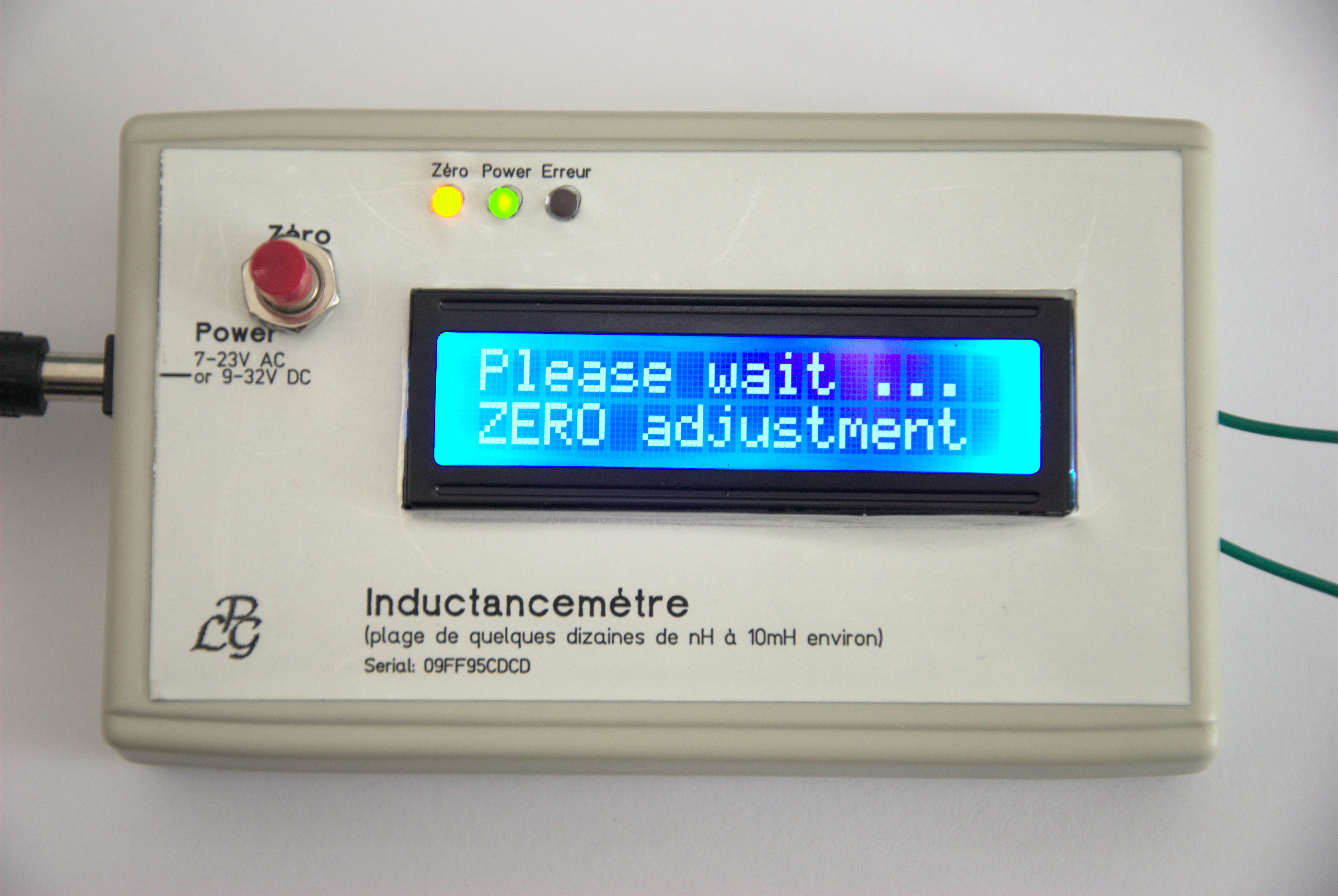
A Modest Inductance Meter
on
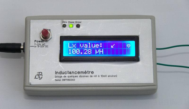
A good instrument to test and measure inductors has been on my lab equipment wish list for many years now, but the cost of such a device has been prohibitive. I therefore decided to build something myself. The little instrument presented here cannot compete with the complex all-singing, all-dancing instruments on the market; it is only a modest inductance meter that enables me to obtain the value of an unknown inductance. There are many of such devices available online, sometimes based on Arduino.
Some years ago, I discovered F. Kudelsko’s website, which describes a small DIY inductance meter capable of measuring inductances from a few tens of nanohenries to approximately 10 mH. A small Windows program retrieves the value of the inductor under test over USB and displays it. Even though I found this approach quite interesting, I was looking instead for a stand-alone device. Yet, I would like to thank the author here for sharing his work on which I based my design.
Principle of Operation
The operating principle of the inductance meter is quite simple. The unknown inductance is used to create an LC oscillator. By measuring the oscillator’s frequency, the value of the unknown inductance can be determined.
There are many ways to build an LC oscillator. Here, a Colpitts oscillator is used (see Figure 1).
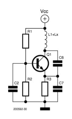
the frequency of the Colpitts oscillator.
The circuit uses a common-base transistor amplifier (Q1) with the input on the emitter and the output on the collector. Without going into details on how this oscillator works, its output frequency is given by the formula of Thomson (a.k.a. Lord Kelvin):
f = 1 / (2π √(LC))
After reworking it, we obtain:
L = 1 / (4π² f²C)
Here C is the value of the two capacitors C6 and C7 in parallel:
C = C6 × C7 / (C6 + C7)
With the value of these capacitors being known — I measured them with my capacitance meter for more precision in the calculations — we only have to plug C into the reworked formula (together with the measured frequency) to find the value of L. It is recommended to use 5% MKT-types.
Inductance Meter Schematic Diagram
The circuit of the inductance meter is shown in Figure 2. I replaced the PIC18F2550 microcontroller in the original schematic with a PIC18F252, as I didn’t need a USB interface, and I added a 2 × 16 alphanumerical LCD. Some component values were determined by what I had available.
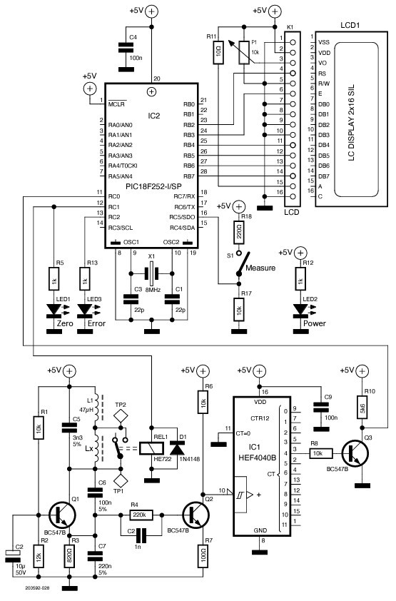
down to something the MCU (IC2) can digest.
Note C5: This part was inherited from the original design [1] and has a slight influence on the oscillator frequency. With C5 the C to use in the calculations is given by:
C = C5 + C6 × C7 / (C6 + C7)
C5 should be of the same precision and quality as C6 and C7.
With my component values (and Lx short-circuited by the relay, see below), the theoretical operating frequency of the oscillator is 83.821 kHz (86.488 kHz with ideal components). Measuring it with an oscilloscope showed a frequency of 88.652 kHz, a difference of 5.4%.
All the calculations are done by the microcontroller. It measures the frequency of the oscillator via its port RC0. For this it is essential to divide the frequency down to values acceptable for the MCU. A 4040-type binary counter (IC1) takes care of this. The division ratio used here is 1/32. I used an HEF4040B for IC1 because that was what I had in stock, but a 74HCT4040 will work too.
L1 and the Relay
To ensure the fast starting of the oscillator irrespective of the value of the unknown inductance Lx, another inductor L1 is placed in series with it. When taking a measurement, the frequency of the oscillator is determined by these two inductances. However, we only want to know the value of Lx. Therefore, the software first takes a measurement with Lx short-circuited. This value, the zero reference, is memorized and used later to calculate the value of Lx.
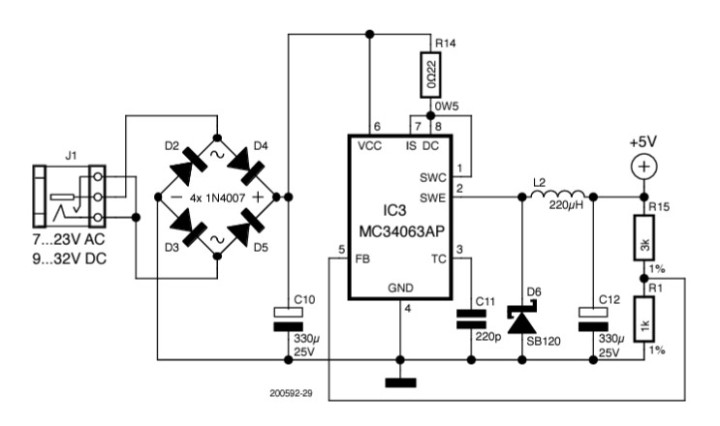
The Power Supply
The power supply is based on an MC34063 (IC3), a switching voltage buck regulator that delivers a nice supply voltage of +5 V (Figure 3). The power source applied to the input of the circuit is first rectified and then filtered by capacitor C10 before entering IC3. The reason for the rectifier D2..D5 is to allow both AC and DC power supplies without having to worry about their polarity. This way the device accepts 7 VAC to 23 VAC or 9 VDC to 32 VDC at its input. Its working frequency is about 30 kHz. The power consumption of the complete circuit is only 35 mA, not a problem for this power supply that can deliver a maximum current of 1.2 A. The power supply connector’s center pin is 2 mm in diameter, which allows for the use of many standard power adapters.
Firmware
I developed a small program in mikroC [2] that, like the original design, allows for the measurement of any inductance, and displays its value (in nH, µH or mH) on the LCD. The measurement range selection is automatic. Measuring the value of Lx is done in two steps:
1. System calibration sequence (relay closed, Figure 4).
2. Measurement sequence with display of the calculated value.
the system calibration sequence.
The MCU’s Timer1 is configured to start counting on the first rising edge on RC0; it will count for one second (controlled by Timer0). After one second, the value of Timer1 represents the frequency of the signal present at its input. Now the processor can perform all the calculations necessary to determine the value of either L1 (Step 1) or Lx (Step 2).
The LCD shows what is going on. During Step 1 the yellow LED (LED1, Zero) lights up. If the inductance to be measured is disconnected, then the message “no coil detected” is shown and the red LED (LED3, Error) will be lit. If this happens, check that the coil is correctly connected and restart the measurement sequence by pressing the push button.
The use of the system is simple and comfortable as it is fully automatic. The only thing to do is to press briefly (approx. 0.5 s) the push button connected to RC5 to restart the procedure if needed. The display shows an arrow to indicate a new measurement.
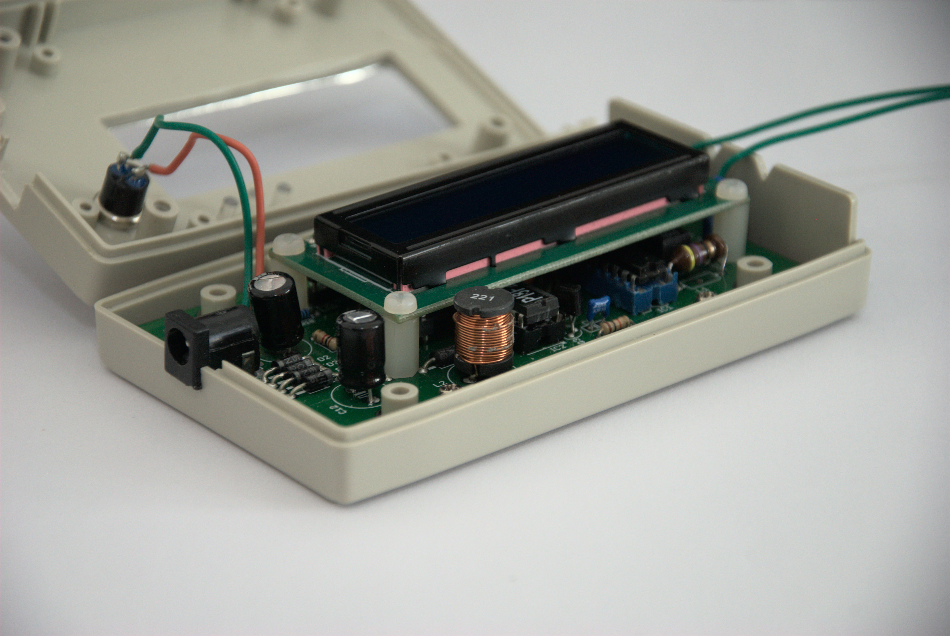
The Building Process
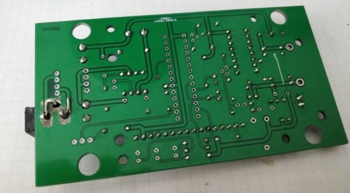
Once the prototype was validated, I designed a double-sided printed circuit board for it. It is intended to fit into a Multicomp MCRH3135 case (Figure 5). Your trained eye may have noticed the small size of the pads. Most of them have a diameter of 1.4 mm for a 0.8 mm hole. I therefore highly recommend using a good soldering iron for mounting the components, or reroute your board differently.
Even though I did my best to come up with a good PCB design, it ended up having two issues that I did not fix:
- I forgot to check the dimensions and the shape of the pads of power connector J1. If you use the same model as I did, you will have to rework the PCB a bit with a Dremel-like tool (Figure 6). As the connector is no longer correctly maintained by its soldered connections, I glued it to the board (after soldering).
- There is no ICSP connector for in-circuit programming of the MCU, which is rather impractical. It is, however, possible to program the MCU by removing it from the board and placing it on a breadboard or prototyping board.
to make the barrel jack fit on its incorrect footprint.
The LCD is mounted on a single-row, 16-way connector, and it is firmly fixed to the PCB with four M3 × 10 mm nylon spacers and suitable bolts and nuts.
The ICs are mounted on sockets which are, of course, not absolutely necessary (unless you want to reprogram the microcontroller...). The relay is soldered directly on the PCB, mainly to avoid unwanted parasitic capacitances and inductances. The three LEDs are soldered almost flush with the PCB, I used light guides (optical fiber) to improve their visibility. The binary file produced by the compiler must be programmed in the microcontroller’s flash memory with a programmer such as the PICkit3.
After designing the front panel using the free Front Panel Designer tool [2][3], I printed it on a self-adhesive aluminum foil (3M) with my laser printer. The result is clean, but cutting the front panel properly and sticking it at the correct position is a bit tricky.
Details and Finishing Touches
It is recommended to keep connections between the device and the inductance-under-test Lx as short as possible because they can introduce errors due to parasitic capacities and inductances. My test leads are 12-cm 0.2-mm² multi-stranded wires with hooks on one end. As for any measuring instrument, switch the device on for a few minutes to stabilize its operating temperature before taking any measurements.
Questions or Comments?
Do you have technical questions or comments about his article? Email the author at pleguen@gmail.com or contact Elektor at editor@elektor.com.
Discussion (2 comments)