
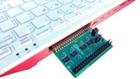
Buffer Board for Raspberry Pi 400 (210320)
28 buffered GPIOs (including GPIO0 and 1) using bi-directional voltage translators. Module for the 40-pin GPIO header in the back
This project is a modification of the Buffer Board for Raspberry Pi 3 and 4 (project 150719, PCB 150719-1), https://www.elektormagazine.com/labs/buffer-boards-for-raspberry-pi-23#. The schematic hasn’t changed but the new PCB is smaller. A right angled receptacle is used for the connector on the Raspberry Pi 400 side of the buffer board (K1) so it can be inserted in the GPIO header in the back. The connector for the buffered IO's is a standard 40 pin male vertical header (K2) Size of the module is 55 x 44 mm, including receptacle K1. Compared to the original PCB 150719-1 the two rows of pins of K1 are swapped, because a receptacle is used here. Placing a standard vertical male 40-way pin header for K1 is not possible. However, this module can still be used with a Raspberry Pi 2 or 3, it then has to be placed upright, but maybe not that practical.
The buffers used are of type TXS0108E and are bidirectional. Each port has a pull-up resistor. The pull-down resistor of a GPIO of the RPi is typically in the order of 40 to 60 kΩ. This value is too high to properly pull down the IO when the buffer board is inserted. The IO’s have a separate power supply for each side, VCCA and VCCB. Every A-port I/O of the TXS0108E has a pull-up resistor to VCCA, connected to the +3.3 V power supply of the Raspberry Pi 400, and each B-port I/O has a pull-up resistor to VCCB. VCCB for the level of the IO’s on K2 can be set to +3.3 V or +5 V logic by jumper JP3. The pull-ups of the buffers have a value of 40 kΩ when the output is driving low and a value of 4 kΩ when the output is driving high. So the outputs of the buffers are in fact open drain. If for instance a led is connected from the output of the buffer to ground a voltage divider is created when an extra series resistor is used. A resistive load on the output will cause the logic high level to drop. Something to keep in mind!
To protect the +5 V and +3.3 V power supply of the Raspberry Pi 400 these are connected from K1 to K2 on the buffer board through 0.5 A PPTC resettable fuses (F1, F2).
For I2C, GPIO2 is SDA1 and GPIO3 is SCL, extra pull-up resistors R1 and R2 can be enable by jumpers JP1 and JP2.
During boot of the Raspberry Pi GPIO0 (ID_SD) and GPIO1 (ID_SC) are used to read an EEPROM of an I2C HAT (Hardware Attached on Top). After boot these GPIO’s can be used like the 26 others, but care needs to be taken if an I2C HAT is mounted the system isn’t affected. To prevent the reading of GPIO 0 and GPIO1 during boot add the following entry to /boot/config.txt:
force_eeprom_read=0
For more information look at the Raspberry Pi Documentation about the config.txt file.
The output K2 can be connected to the external circuit through a short 40way ribbon cable with two 2x20 receptacle connectors attached or just a single receptacle with short wires soldered to them or single sockets with wires. But be careful pressing a 40 way receptacle onto K2, or removing it from the board. Don’t do this while the buffer board is still inserted in the Raspberry Pi 400 because a lot of force is needed and the GPIO header of the Raspberry Pi 400 could get damaged otherwise.
Two very minimal python programs from the original project are attached. One is to test all GPIOs as output, Check_all_GPIOs_as_output.py, and the other is to test all GPIOs as input, Check_all_GPIOs_as_input.py (210320-11.zip). In Raspbian just double click on one of the files and the default IDE for Python will open. Select RUN. When testing the GPIOs as output only a single low current LED is needed. Outputs are tested in group of eight maximal. As a series resistor for the LED a 1.8 kΩ resistor can be used, but the value is not that critical. It will prevent damaging the LED if connected to the plus directly. Because of the open drain output the voltage across a LED (red) plus resistor is about 2.6 V, when 5 V is selected as a power supply for the outputs (JP3). Connect the resistor plus LED to one of the chosen outputs and it wild light 0.2 seconds and 7 times that stay off because the 8 outputs are set high 0.2 s and low again sequentially. Change ‘IOA’ to one the other groups in the line
for i in IOA: # leds blink 0.2 s in IOx group
to test the other groups of outputs. Of course GPIO0 and GPIO 1 can be added to group IOA.
The program to test the GPIOs as input uses one IO as output, GPIO3. Connect a 1,8 kΩ resistor and LED (pin 5). An input is selected one at the time to make sure only this one is working as input. Change the number in the following line to test an other GPIO:
IN1 = 2 #selected GPIO to test as input
Finally change the GPIO set as output to another one to also check GPIO3 as input. The program also prints the selected GPIO and its input level. The inputs have their pull-ups enabled. So to make the connected LED light the current input pin must be connected to ground. When done so the printout will change. Of course there are numerous ways to test the GPIO’s, if anyone has a more efficient and/or faster way please share.
Bill of materials
Resistor
R1,R2 = 10 kΩ, 100 mW, 1 %, SMD 0603
Capacitor C1-C8 = 100 nF, 50 V, 10 %, X7R, SMD 0603
Semiconductor
IC1-IC4 = TXS0108EPWR, SMD TSSOP-20
Other
K1 = 2x20 receptacle, right angle, pitch 2.54 mm
K2 = Pin header, 2x20, vertical, pitch 2.54 mm
JP1,JP2 = 2-way pinheader, vertical, pitch 2.54 mm
JP3 = 3-way pinheader, vertical, pitch 2.54 mm
JP1,JP2,JP3 = Shunt jumper, 2.54 mm spacing
F1,F2 = PPTC Resettable Fuse, SMD, polyfuse, 1210L050YR Littelfuse
Misc.
PCB 210320-1 v1.0
Raspberry Pi – 40-pin GPIO header
1 3.3V
2 5V
3 GPIO2 (SDA1)
4 5V
5 GPIO3 (SCL1)
6 GND
7 GPIO4
8 GPIO14 (TXD0)
9 GND
10 GPIO15 (RXD0)
11 GPIO17 (GPIO_GEN0)
12 GPIO18 (GPIO_GEN1)
13 GPIO27 (GPIO_GEN2)
14 GND
15 GPIO22 (GPIO_GEN3)
16 GPIO23 (GPIO_GEN4)
17 3.3V
18 GPIO24 (GPIO_GEN5)
19 GPIO10 (SPI_MOSI)
20 GND
21 GPIO9 (SPI_MISO)
22 GPIO25 (GPIO_GEN6)
23 GPIO11 (SPI_SCLK)
24 GPIO8 (SPI_CE0_N)
25 GND
26 GPIO7 (SPI_CE1_N)
27 GPIO0 (ID_SD)
28 GPIO1 (ID_SC)
29 GPIO5
30 GND
31 GPIO6
32 GPIO12
33 GPIO13
34 GND
35 GPIO19
36 GPIO16
37 GPIO26
38 GPIO20
39 GND
40 GPIO21
GPIO# pin
GPIO0 27
GPIO1 28
GPIO2 3
GPIO3 5
GPIO4 7
GPIO5 29
GPIO6 31
GPIO7 26
GPIO8 24
GPIO9 21
GPIO10 19
GPIO11 23
GPIO12 32
GPIO13 33
GPIO14 8
GPIO15 10
GPIO16 36
GPIO17 11
GPIO18 12
GPIO19 35
GPIO20 38
GPIO21 40
GPIO22 15
GPIO23 16
GPIO24 18
GPIO25 22
GPIO26 37
GPIO27 13
Discussion (0 comments)