
DDS Function Generator Shield for Elektor FPGA Board (140006-I)
After going through the recent Elektor FPGA Board article series, I wanted to put my FPGA board to some practical use while gaining more experience in VHDL programming, learning by doing.
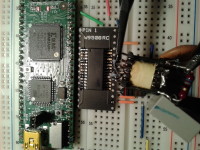
The first primitive prototype shows the DAC (TI DAC904) mounted on a converter base for breadboard pin scale, along with a primitive output circuit for the DAC. I envision the final layout to mount either under the FPGA board or perhaps over it with minimal intrusion to the the FPGA board itself.
The oscilloscope bottom traces show the signals taken directly at the DAC output, and the upper traces show the same signals taken at the output side of the circuit output transformer (PT8SM).
The DAC904 can run at up to 200 MSPS, but I seem to be getting better trace results running at 112 MSPS. I need to do more experimenting with accumulator size and internal sync frequency.
I am not very concerned as yet with the unsymmetrical low frequency (8 kHz) square wave, since this is the first feasability test with a not very well balanced output circuit. Also, no separate power for digial and analog as yet. I wanted just a quick proof of concept before doing any serious fine tuning.
At 500 kHz one can see the quantisizing noise in the bottom traces, which are largely filtered out in the upper traces.
At 50 MHz the signal seems to be getting out of hand. Not sure if that can be managed or not. More testing needed. Also not sure how much of the problem relates to deficiencies in my oscilloscope and/or probes.
UPDATE 1 MARCH 2014: I have added a trace at 80 MHz after adjusting internal sync frequency to 128 MHz. Considering the crude test layout, I am not too dissatisfied. I notice that the Xylinx chip gets quite warm while running internally at 128 MHz using my code.
I have also modified the VHDL code to include pushbuttons for increasing/decreasing output frequency, and have successfully tested this on the hardware.
Now also added pushbuttons for wave form selection and successfully tested on hardware. This did not want to work right off, and then I realized that the FPGA internal pulldown settings for the pushbutton input ports were not getting the job done as expected. I therefore had to add external pulldown resistors on the FPGA pins, after which everything worked like a charm. I have added 2 additional photos showing a 270 kHz signal trace switching from sine wave to sawtooth using wave select buttons.
I will publish the VHDL source code as soon as I get written approval from Elektor-Verlag GmbH.
UPDATE 2 MARCH 2014: I have added my VHDL code for the frequency setting module. This module is a part of my modifications to the basic DDS generator which was inspired by Elektor-Verlag publication "Hardware-Design mit FPGA" in chapter 7 as a practical example for VHDL programming. In my adaptation, I am using a 31 bit accumulator, a 14-bit DAC, and a lookup table (LUT) containing an array of 4x16384 encompassing 4 14-bit waveform hex values (file WAVEHEX14.ZIP) for representing the sine, sawtooth, triangle and square waves. I generated the hex values using a spread sheet (file sinehex.zip) and a small qbasic programm. During testing I discoverd that I must not use hex value 0x0000, since the DAC will not produce square wave output using 0x3FFF for HIGH and 0x0000 for LOW, but does work with 0x3FFF for HIGH and 0x0001 for LOW.
UPDATE 9 MARCH 2014: Progress continues. Pushbutton-debounce VHDL module now tested and working on the hardware. This is a modifed version of the debounce module for the FPGA extension board published in Elektor Jan/Feb 2014 issue, but adapted to handle 8 pushbuttons plus the correction of an error in the original which was preventing the module from sending its signal for exactly 1 clock period as specified (the original code sent each pushbutton signal continuously for 4 ms instead of only 1 clock cycle). Also added and tested a VHDL module which determines the step sizes required to increment/decrement frequency in units, thousands and millions as well as the factors x10 and x100. The step size is then fed to module "step", which then drives the frequency of the DDS module. I also added an addional pushbutton to be used to enable increasing/decreasing the frequency at the highest step resolution (0.0588 Hz at 128 MHz sync frequency which I am currently testing). No problems encountered in producing signals from 0 Hz to 10 MHz. Above 10 MHz the DAC is producing spurious waveform distortions at various frequencies, which I still need to resolve (not yet sure how).
UPDATE 11 MARCH 2014: I have now received formal approval from Elektor-Verlag to publish here my code which is based on intellectual property of Elektor-Verlag. However, before I do actually publish that code, I need to understand just what I must do to properly publish as "Open Source". I will publish as soon as possible. Please be patient with me.
Since the problems I have encountered with waveform distortions at frequencies above 10 MHz occur at DAC output frequencies well below the Nyquist frequency (64 MHz @ 128 MHz sample rate), I am now assuming that they are coming from noise introduced into the DAC clock input line and/or power inputs as a result of my primitive circuit.
I am currently testing VHDL module enhancements for signal sweep. Hope to publish soon.
UPDATE 16 MARCH 2014: Added new zip file (DDSFGen4FPGA.zip) containing all modules currently implemented and tested on hardware. These files are submitted as open source under GPL license and can be used to create an FPGA project in Xylinx Project Navigator. Also included is the binary compilation (config.bin) of the current development state. This binary can be copied to an SD card and loaded directly into the Elektor FPGA board. For pin connections between the Elektor FPGA board and the external push buttons and DAC, see the Top.ucf file. Please note that if you create a project in Xylinx Project Navigator using these files, the compilation time can take up to 2 hours, primarily due to the large LUT array.
Module enhancements for signal sweep are still under construction.
UPDATE 23 MARCH 2014: I managed to get signal sweep enhancement to work (screenshots uploaded), but only with the waveform LUT array reduced to sine wave only. When I attempt to implement with the full 4-waveform array, the FPGA resources are exhausted and the circuit does not fit into the FPGA. I tried reducing the LUT to 3 waveforms (sine, sawtooth and triange) and program square wave using if-else statements. Also tried removing reset button logic and also maximum resolution button logic, also reduced input arrays accordingly, but none of these measures reduced resource usage enough to get the circuit to fit into the FPGA. It looks like I will have to abondon the signal sweep option, or perhaps resolve by using alternative programm versions. For now I will pass over this issue and move on to next issue (add LCD module).
UPDATE 26 MARCH 2014: I have solved the resource usage problem. My original design was set up with a 32-bit size accumulator, which I reduced to 31-bit size somewhere during my attempts to get the circuit to run on the hardware. Back-tracking, I found that simply reducing the accumulator from 32-bit size to 31-bit size caused the FPGA slice utilization to jump from 61% up to 99%. I am guessing that this, for me rather surprising, behaviour is related to the "powers of 2" VHDL mathematics which I am unaccustomed to and which has caused me unending hours of rework action right from the beginning of this project. In any case, I have now set the accumulator back to 32-bit size. The circuit still works on the hardware, and the FPGA is back down to "only" 64% slice utilization. That should give me enough free resources to complete the design, including signal sweep functionality. :) Lesson learned: avoid non-"power of 2" sized vectors whenever feasible. ;)
UPDATE 13 APRIL 2014: Although I have nothing good to report, I felt it was time to provide an update. My previously reported optimisum in regard to solving the FPGA resources problem was premature. After a closer look at the generated waveforms, I realized that the change from a 31 bit accumulator size to 32 bit resulted in lower FPGA resource consumption because apparently only half of the LUT circuitry was actully getting programmed. Although the config file genererated without errors and the simulation looks good, the actual hardware results show distortion in the second half of each waveform. In the meantime I have tried reducing the LUT size from 14 bit to 13 bit, but I am not satisfied with the resulting decrease in usable frequency range (unacceptable waveform distortion above ca. 10 MHz). I will now persue the suggestion of Clemens to use a CORDIC-algorithm to generate sine waves. I expect this to take a while, so do not expect further updates very soon. Sorry.
Open issues:
- Continue adding and hardware testing of VHDL peripheral modules from the original concept (BDC frequency converter module and LCD output of frequency and wave form).
- Resolve FPGA resource over-utilization problem
- Resolve spurious waveform distortions occurring above 10 MHz.
- Create first draft of the layout for the DAC/output circuit PCB
- Finalize enhancing VHDL accumulator module to handle signal sweep
- Document module design and usage
More to come...
References:
http://www.elektor.de/products/kits-modules/modules/-(-91)/120099-91-taming-the-beast.2316953.lynkx
http://www.elektor.de/products/books/e-books/hardware-design-mit-fpga.2648131.lynkx
Build This Project
Bring this design to life with the Elektor PCB Service, powered by Eurocircuits. Upload the project files and order professionally manufactured PCBs or assembled boards through a proven European production platform.
Supporting KiCad, Eagle, Gerber, and ODB++ formats, the service is suitable for everything from prototypes and validation builds to series production and volume manufacturing.
Made in Europe. Fast. Reliable. Professional.
Discussion (2 comments)