
Microphone Preamplifier with Transformer and Phantom-Power [140426]
High performance microphone preamplifier with phantom power for use with line-level audio inputs as found on todays computers. Gain can be set in six steps from 20 to 70 dB, 20 dB by 1: 10 input transformer.
By Joseph Kreutz (translated from French)
Apparently outdated, the transformer is used to design a simple circuit, having furthermore an effective electrical isolation of the input and good rejection of the common mode signal. It contributes substantially to the reduction of interference, such as those caused by mobile phones. Microphone transformers with a ratio of 1:10 are not hard to find. They raise 20 dB signal voltage, which contributes to a significant improvement compared preamp signal to noise. These performances require the selection of an operational amplifier FET whose input noise current is negligible.
Despite its price, the ultimate would be to have a AD743, distinguished by its remarkably low input noise of 2.9 nV/√Hz [1]. Thru moderate cost, the OPA 134 model produced by Texas Instruments (former Burr Brown) is an excellent choice, and ... the preamp prototype was made based on a TL071 with a surprisingly good result. [2] The dual operational amplifiers such as TL072 or OP2134 models perfectly suit stereo achievements.
Obtaining transformers poses little difficulty. For example, the German company Bürklin [3] distributes, which for a reasonable price offer very acceptable quality. The firms Lundahl [4] Sowter [5] and Jensen [6] provide production-quality products, but substantially more expensive. A visit to the "Web" should certainly reveal other interesting prospects.
FIG. 1 shows the preamplifier scheme. The signal from the microphone is applied to the primary of transformer T1. Connecting the said microphone will preferably by a connector XLR to usual standards in the professional field, or a "jack" stereo 6.35 mm. In this case, the connector end is at the hot spot, the intermediate ring at the cold spot and the remaining part of the mass. Condenser microphones require the application of a supply voltage of +48 V. This is what is intended resistors 6.8 kΩ, the exact value is not of paramount importance, but must be matched with an accuracy of 0.4% or better [7, 8]. You may need to select the ohmmeter. They should be capable of dissipating 0.5W at least to avoid grilling when shorted to ground. One connection of the secondary of transformer T1 is connected to ground, on the other to the non-inverting input of the operational amplifier IC1, whose inverting input is connected to the feedback network which will determine the gain of the preamplifier. The 6 position rotary switch allows to establish a direct connection between the output and the inverting input of the operational amplifier, or progressively connecting resistors R6 to R10 in series. Each step results in a gain increase of 10 dB. As the transformer already provides a gain of 20 dB, the preamplifier will therefore produce a gain between 20 and 70 dB. Whenever possible, the switch should be of the type "make before break" which bypasses the contacts during his maneuver to avoid sudden gain jumps. Capacitors in parallel with R6 to R10 serve to limit the bandwidth of the preamplifier at 32 kHz.
100 nF decoupling capacitors C3 and C4 should be installed as close as possible to the operational amplifier. The resistors are preferably metal film components with a tolerance of 1%. This choice is necessary also for R5 to R10. Resistor 470 kΩ R4 can be omitted if the microphone is not to be charged by a particular impedance. Otherwise, choose a value of up to a hundred times the recommended impedance. The electrolytic capacitors should withstand a voltage of 25 V, with the exception of C1, which must be a model 63 or 80 V. The supply voltages of the operational amplifier are hardly critical insofar they correspond to the specifications of the manufacturer.
If we restrict the use of electrodynamic microphones that do not require 48V, C1 and R1 to R3 components are obviously not required.
The fixed computers all produce voltages of +12 and -12 V exploitable for the preamplifier supply. If this source is used, it will be necessary to carefully filter: these tensions are likely to be heavily polluted by the noise generated by the motherboard and other digital equipment. It will also be wise to incorporate slow fuse of 100 mA in each of the supply lines to avoid damaging the computer incidentally.
References.
[1] http://www.analog.com
[2] http://www.ti.com
[3] https://www.buerklin.com (English and German)
[4] http://www.lundahl.se/our-products/microphones/
[5] http://www.sowter.co.uk/pro-audio-transformers.php#
[6] http://www.jensen-transformers.com/mic_in.html
[7] Jörg WUTTKE
"Mikrofonaufsätze" p. 83
SCHALTTECHNIK Dr- Ing SCHOEPS GmbH
Spitalstraße 20
D-76227 KARLSRUHE - Germany
www.schoeps.de
(German Document downloadable site of the aforementioned firm - Worth to be read)
[8] DIN EN61938 Standard
Instead of a bridge rectifier for the symmetrical 12 V supply we used 4 1N4007. It’s much more universal, cheaper and there’s less chance having a bridge rectifier with the wrong pinout. For the +48 V supply we used a transformer with two secondary windings of 24 V. This way there’s no need for a voltage doubler and only one big smoothing capacitor is needed. As you can read in the text from Joseph the 48 V has a margin of +/- 4 V. In our prototype the output voltage was 50.6 V unloaded. It complies with the standard. Changing R8 to 93.1 kΩ (E-96) reduced the output voltage to 48.04 V. That is of course only the case for this particular prototype. Now you know which resistor to change if the output voltage is too far off. Both transformers have two primary windings so the power supply can be used with mains voltages of 115 V and 230 V. For 230 V only 1 jumper wire must be placed for JP1 and two for 115 V. Three is not possible. It’s clearly marked on the PCB. In case 115 V mains voltage is used the fuse rating must have the double value. The manufacturer only recommends secondary fuses for each transformer but for extra safety we added one primary also, just to be sure. Current consumption of the OPA134 is only 5 mA max. at TA = +25°C. So the 7812 and 7912 don’t need a heat sink, not even when two amplifiers are connected. The dissipation of the +48 V regulator, so T1 in particular, is mainly caused by the high input voltage and the reason to mount T1 onto a heat sink. It’s small but a thermal resistance of about 20 °C/W is more than enough cooling. The rectified secondary voltage of TR2 without a load at the +48 V output is more than 85 V. Together the two secondary voltage in series deliver 61.6VAC! With a load of 10 mA the output voltage drops to 47.6 V and the input of the regulator to 80 V. If a 1 kΩ resistor is connected to the +48 V the voltage drops to about 46.6 V and the input to 66 V. Latter causes a dissipation of 0.9 W in T1. The maximum dissipation occurs when the output is short circuited. The short circuit current in our prototype was 52.5 mA (0.63 V over R6, ignoring the bias current of T3). The voltage at the input of the regulator dropped to 66 V. In case of a prolonged short circuit on the +48 V power supply the maximum dissipation of T1 is about 3.4 W continuously. But this will probably never happen. With the chosen heatsink this means a junction temperature of close to 100 °C. This is tolerable but doesn’t do the TIP31C any good. For a long life span the junction temperature of a semiconductor should be kept below 70 °C. Measured ripple is less than 0.2 mVpp at 10 mA. It’s suppressed even more on the amplifier board.
There’s not much to say about the +/- 12 V power supply. It’s pretty standard. The power rating of the transformer used is more than enough for the few mA’s one or two amplifiers will need. The amplifier connected the input voltage of the two regulator is about +/- 26.2 V. This is much higher than needed and a 2VA/2 x 12 V transformer can be used to keep the input voltage in a safer range. Because of the light load secondary voltages of the 4VA/2x15V transformer are each 20.3 V! The two transformers we used are more likely to be found at various distributors.
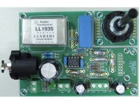
Maybe the most important part of the amplifier PCB is the fact that three different microphone transformers can be used for TR1. Lucky for us the footprints of the three transformers from Pikatron (ÜP3095M, ÜP3096M), Lundahl (LL1935) and Jensen (JT-115K-EPC) can be combined into one footprint and still connect all three the proper way. The Lundahl LL1935 transformer has 2 primary and two secondary windings that can be used the other way round (specifically stated in the datasheet but probably also true for the other transformers). The schematic symbol used for all three is a compromise and doesn’t show the real connections of a single one of the transformers. Confused? The Pikatron ÜP3095M (pin 1 indicated by a painted dot on the side) has one primary and one secondary winding in a turns ratio 1 : 10 and a separate ground pin. The Lundahl LL1935 transformer has two primary and two secondary windings in turns ratio 1 + 1 : 5 + 5 and a separate ground pin. The ground pin is place asymmetrically and the transformer can only fit one way. The Jensen JT-115K-EPC transformer has one primary and one secondary winding in turns ratio 1:10 and two ground pins between the pins of the secondary winding. All pins of the three transformers are located in such way no overlap in placement of the connected pads take place when the centers of the transformers are aligned. The pads are numbered according the schematic symbol in such way that the connections are conform a 1 :10 turns ratio for all three transformers. Be careful when using the Pikatron transformer. The metal case can short the connections of the Jensen transformer and thereby its own connections. When soldering the pins keep it little bit hovering above the PCB or put half a millimeter thick insulating material underneath the transformer.
A project update about putting the two PCBs in their respective enclosures will soon follow.
Maximum output voltage 7.8 V (THD 0.1 %, gain 70dB)
1 kHz, 1 V out, B 22 kHz referred to 1 V out, B 22 kHz low / high
20 0.0032 % 110 dB / 112.7 dBA < 10 Hz / 74 kHz
30 0.0014 % 100 dB / 103 dBA 12.2 Hz / 37 kHz
40 0.0028 % 90.8 dB / 93.1 dBA 12.8 Hz / 34 kHz
50 0.0087 % 80.8 dB / 83 dBA 12.8 Hz / 34 kHz
60 0.027 % 71 dB / 73 dBA 12.8 Hz / 30.6 kHz
70 0.078 % 62 dB / 63.5 dBA 12.8 Hz / 17 kHz
1 kHz, 1 V out, B 22 kHz referred to 1 V out, B 22 kHz low / high
20 0.0034 % 109 dB / 112 dBA < 10 Hz / ? (>200 kHz)
30 0.0016 % 100 dB / 102 dBA 14.5 Hz / 30 kHz
40 0.0031 % 90.6 dB / 92.6 dBA 15.3 Hz / 28.3 kHz
50 0.0097 % 80 dB / 82.2 dBA 15.3 Hz / 26.2 kHz
60 0.030 % 70.4 dB / 72.5 dBA 15.3 Hz / 23.3 kHz
70 0.086 % 61.1 dB / 62.7dBA 15.3 Hz / 16.2 kHz
We also recorded some plots with our Audio Precision Analyzer
Lundahl LL1935:
Plot A (AMP_Lundahl_1) shows amplitude versus frequency from 10 to 200 kHz for all gain settings. From top to bottom the cyan, green, yellow, red, magenta and blue plot correspond to 70, 60, 50, 40, 30 and 20 dB total gain respectively. At 20 dB the plot is practically the curve from the transformer. IC1 acts pure as a buffer. At 151 kHz there’s a resonance peak of which amplitude and frequency largely depend on the source impedance and sort of source (single ended or balanced). At gains of 30, 40 and 50 the high cut-off frequencies are more or less the same but at 60 and 70 dB unity gain bandwidth of the opamp is beginning to show. At a gain of 50 dB bandwidth of the OPA134 is 8 MHz/316 is 25.3 kHz! If more bandwidth is desired at the highest gains maybe a LME49710 (GBW 55 MHz) or an OPA627 (GBW 16 MHz) is an option. Changing C5 to 22 µF will lower the cut-off frequency to 9.6 Hz and de relative gain at 20 Hz from -1.48 dB to -0.87 dB.
Plot B (THDvsFRQ_1V_Lundahl_1) shows distortion plus noise versus frequency at 1 V output voltage and all gain settings at a bandwidth of 80 kHz. To maintain the same output voltage at every gain setting the level of the input signal is increased accordingly. The same color/gain scheme as previous plot is kept here. At the highest gain just an input level of 335 µV is needed for an 1 V output signal. At the highest gain it’s mainly noise but as with lower gain settings the input voltage increases distortion becomes the main factor. The increasing distortion at the low and high end of the plots at higher input levels is caused solely by the transformer.
Plot C (THDvsLVL_Lundahl_2) shows distortion plus noise versus output level at 1 kHz and a bandwidth of 22 kHz. Only at the two highest gain settings does distortion rise again towards the end of the plots.
Plot D (FFT_1V_20dB_Lundahl_1) shows an FFT of 1 kHz at the lowest gain setting (20 dB total) and 1 V output voltage. Mainly a third harmonic at -90 dB is responsible for the total harmonic distortion plus noise result of 0.0032 %.
Plot E (FFT_1V_70dB_Lundahl_1) shows an FFT of 1 kHz at the highest gain setting (70 dB total) and 1 V output voltage. Since all frequencies (read noise) are close to a level of 90 dB total harmonic distortion plus noise sums up to 0.078 %.
Pikatron ÜP3095M:
Plot F (AMP_UP3095M_1) shows amplitude versus frequency from 10 to 200 kHz for all gain settings. A resonance peak is just beyond 200 kHz. Total bandwidth is less than is the case with the Lundahl transformer but for all practical purposes good. Replacing C5 with 22 µF lowers the low cut-off frequency from 15.3 to 12 Hz.
Plot G (THDvsFRQ_1V_UP3095M_1) shows total distortion plus noise versus frequency at 1 V output voltage and all gain settings at a bandwidth of 80 kHz. Only at the lowest frequencies is total distortion plus noise higher than using the Lundahl transformer.
Plot H (THDvsLVL_UP3095M_1) shows distortion plus noise versus output level at 1 kHz and a bandwidth of 22 kHz. It’s hard to tell the difference with the Lundahl plot. Levels are marginally higher.
Plot I (FFT_1V_20dB_UP3095M_1) shows an FFT of 1 kHz at the lowest gain setting (20 dB total) and 1 V output voltage. The third harmonic is the main factor and the rest of the harmonics are a bit higher compared to plot D. Total harmonic distortion plus noise of this spectrum is 0.0034 %.
Plot J (FFT_1V_70dB_UP3095M_1) shows an FFT of 1 kHz at the highest gain setting (70 dB total) and 1 V output voltage. A third harmonic is barely visible and the rest is just noise. This spectrum corresponds to a total harmonic distortion plus noise of 0.086%
Resistor
R1 = 220 Ω, 1 %, 250 mW, metal film
R2,R3 = 6.8 kΩ, 0.1 %, 500 mW, metal film
R4 = 470 kΩ, 1 %, 400 mW, metal film
R5 = 1.0 kΩ, 1 %, 600 mW, metal film
R6,R12 = 2.2 kΩ, 1 %, 400 mW, metal film
R7 = 6.8 kΩ, 1 %, 400 mW, metal film
R8 = 22 kΩ, 1 %, 250 mW, metal film
R9 = 68 kΩ, 1 %, 250 mW, metal film
R10 = 220 kΩ, 1 %, 250 mW, metal film
R11 = 47 Ω, 1 %, 250 mW, metal film
R13 = 12 kΩ, 1 %, 250 mW, metal film
R14,R15 = 22 Ω, 1 %, 250 mW, metal film
Capacitor
C1 = 220 µF, 100 V, 20 %, lead spacing 5/7.5 mm, diam. 17.8 mm max.
C2 = not mounted
C3,C4 = 100 nF, 100 V, 5 %, lead spacing 5/7.5 mm, PET
C5 = 15 µF, 63 V, 10 %, lead spacing 5/7.5/10/15/22.5 mm, PET
C6 = 2n2, 1 %, 160 V, lead spacing 5/7.5/10/14.6 mm, polystyrene, axial
C7 = 680 pF, 2.5 %, 160 V, lead spacing 5/7.5/10/14.6 mm, polystyrene, axial
C8 = 220 pF, 2.5 %, 160 V, lead spacing 5/7.5/10/14.6 mm, polystyrene, axial
C9 = 68 pF, 2.5 %, 160 V, lead spacing 5/7.5/10/14.6 mm, polystyrene, axial
C10 = 22 pF, +/- 1 pF, 160 V, lead spacing 5/7.5/10/14.6 mm, polystyrene, axial
C11,C12 = 220 µF, 50 V, 20 %, lead spacing 5 mm, diam. 10 mm max.
Transformer
TR1 = LL1935, 1:10 (1 : 1 : 5 + 5), Lundahl, 38 x 23 x 16 mm
Semiconductor
LED1 = LED, green, 3 mm, T-1
LED2 = LED, blue, 3 mm, high intensity, T-1
IC1 = OPA134PAG4, DIP-8
Other
K1 = XLR Audio Connector, 3 Contacts, Socket, PCB Mount (Neutrik NC3FAAH1)
K2,K4 = Terminal block 5.08 mm, 2-way, 630 V
K3 = Terminal block 5.08 mm, 3-way, 630 V
K5 = 7-way pinheader SIL, pitch 2.54 mm, right angle, or simply short wires
K6,K7 = not mounted (opposite side of K5)
S1 = Rotary switch, 2 pole 6 position, PCB terminals, MBB, Lorlin CK1060
Misc.
PCB 140426-1 v1.1
PCB designed for enclosure 1455K1201, Hammond Manufacturing
Alternative microphone transformers that will also fit on the PCB
TR1 = Pikatron ÜP 3095 M, 1 : 10, (available at www.buerklin.com), 18 x 14.5 x 13.2 mm
TR1 = Pikatron ÜP 3096 M, 1 : 15, (available at www.buerklin.com), 18 x 14.5 x 13.2 mm
TR1 = Jensen transformers JT-115K-EPC, 1 : 10, 31.75 x 31.75 x 23.62 mm
http://www.jensen-transformers.com/transformers/mic-input/
Resistor
R1 = 2.2 kΩ, 5 %, 0.25 W, carbon film
R2 = 1.0 kΩ, 1 %, 0.6 W, metal film
R3 = 39 kΩ, 1 %, 0.25 W, metal film
R4 = 22 kΩ, 1 %, 0.25 W, metal film
R5 = 68 Ω, 1 %, 0.4 W, metal film
R6 = 12 Ω, 1 %, 0.25 W, metal film
R7 = 470 Ω, 1 %, 0.25 W, metal film
R8 = 100 kΩ, 1 %, 0.25 W
R9 = 33 kΩ, 1 %, 0.25 W
Capacitor
C1,C3,C5,C7,C14,C17 = 100 nF, 100 V, 5 %, lead spacing 5/7.5 mm, PET
C2,C6 = 10 µF, 50 V, 20 %, lead spacing 2 mm, diam. 6.5 mm max.
C4,C8 = 2200 µF, 50 V, 20 %, lead spacing 5/7.5 mm, 17.8 mm max.
C9,C10,C11,C12,C19,C20,C21,C22 = 10 nF, 200 V!, 10 %, lead spacing 5.08 mm, ceramic X7R
(C322C103K2R5TA, Kemet)
C13,C16 = 220 µF, 100 V, 20 %, lead spacing 5/7.5 mm, 17.8 mm max.
C15 = 15 nF, 100 V, 5 %, lead spacing 5/7.5 mm
C18 = 470 µF, 100 V, 20 %, lead spacing 5/7.5 mm, 17.8 mm max.
C23,C24 = 100 nF, X1, 440 VAC, lead spacing 10/12.5/15 mm, polypropylene
Inductor/Transformer
L1 = B82724J2142N1, choke, common mode, 2x27mH, 1.4A
TR1 = FL4/15 Block, prim. 2 x 115V, 2 x 15 V sec., 2 VA, PCB mount
TR2 = FL6/24 Block, prim.2 x 115V, sec. 2 x 24 V, 6 VA, PCB mount
Semiconductor
D1,D2,D3,D4,D5,D6,D7,D8,D9,D10 = 1N4007, 1000 V, 1 A, DO-41
D11 = 1N4148, 100 V, 200 mA, DO-204AH
D12 = BZX55C12, zener diode 12 V/0.5W, DO-35
Other
JP1 = 0.6 mm wire (see text)
K1 = Terminal block 5.08 mm, 3-way, 630 V
K2 = Terminal block 5.08 mm, 2-way, 630 V
K3 = Terminal block 7.62 mm, 2-way, 630 V
F1,F2,F3,F5(*1) = Fuse, 100 mA, time delay, 250 V, 20 x 5 mm
F4 = Fuse, 160 mA, time delay, 250 V, 20 x 5 mm
F1,F2,F3,F4,F5 = Fuse holder, 20 x 5 mm, 500 V, 10 A
F1,F2,F3,F4,F5 = Cover for fuse holder 20 x 5 mm
HS1 = Heat sink SW25-4 Aavid Thermalloy, 13 °C/W, 34.5 x 12.5 x 25 mm
Misc.
PCB 140426-2 v1.0
*1 for 115 VAC F5 = 200 mA, time delay, 250 V, 5 x 20 mm
PCB designed for HAMMOND 1455N1601 Enclosure
The enclosure of the microphone amplifier takes more work. In the front panel a hole at exactly the correct place has to be made for the 3pole XLR microphone connector K1. It’s soldered onto the PCB and can’t be moved. All other holes in the panels have some tolerance where they should be located. Located to the right of K1 is the power on led. It is connected to the PCB with thin stranded wires soldered directly the PCB. LED2 indicating the presence of the Phantom Power is only useful if it can be switch off (e.g. a switch in series with K4). In our prototype the Phantom Power is permanently connected and LED2 is not put on the front panel. We used the smaller PCB to connect the rotary switch but another option is to simply connect wires directly from the rotary switch to the amplifier PCB. Also other rotary switches (better quality) can be used this way. The rotary switch is mounted in the back panel at half height at a position for shortest connections (see photo). Connections from the rotary switch to the amplifier PCB are made by thin stranded wires soldered at both ends directly to the PCB. The rotary switch has a plastic locking pin piercing the panel to prevent the whole switch from turning. Make use of it. Locating the correct position for this pin however is a little difficult. The datasheet from Lorlin shows panel mounting piercing details. The rotary switch used (see BOM) is make-before-break. Turning a break-before-make rotary switch will cause gain to be temporarily maximal and can cause acoustic feedback. The power supply voltages are connected by a 5pole male XLR connector. This way the connecting cable has a female connector and there’s less chance shorting the cable connector. For all power supply connections 0.75 mm2 stranded wires were used. The cable we used contains 4 wires and a shield. The shield was used for the ground connection of the +/- 12 V supply. The output connector is a RCA (Phono) connector located left of the XLR microphone connector and just above the Lundahl transformer. This connector also takes care of grounding the metal enclosure. To connect the output connector two twisted thin stranded wires can be used but a short piece of high quality shielded audio cable is maybe better.
Power supply:
female XLR Neutrik NC5FD-LX, panel mount (Farnell 1390124)
male XLR Neutrik NC5MX, cable mount (Farnell 250764)
Microphone amplifier:
Male XLR Neutrik NC5MP, panel mount (Farnell 250820)
Female XLR Neutrik NC5FXX, cable mount (Farnell 1108204)
Cable:
we used Pro Power PPCY4C0.5 (per meter), screened, 4 cores 0.5 mm2, outer diameter 6.5 mm or consider Pro Power PPCY4C0.75 (per meter), screened, 4 cores 0.75 mm2, outer diameter 7 mm
The amplification circuit
Described here are two reasons for the development of the preamplifier. It has been a long time since tape recorders have fallen into obsolescence. So a substitute has to be found: for example, a laptop equipped with a USB sound card. Nowadays desktop computers virtually all have a line input of generally acceptable characteristics. Their microphone inputs exhibit noise and distortion levels that are rather poor, and are only mono. They are not suitable for professional microphones with a balanced output, which often also require a "phantom" power of +48 V. The idea is to achieve a high performance preamplifier that can be connected to the line input of computers and allows to circumvent the problems that were mentioned. The high end card owners will not necessarily be the only ones to appreciate the true value of the use of such a preamplifier.Apparently outdated, the transformer is used to design a simple circuit, having furthermore an effective electrical isolation of the input and good rejection of the common mode signal. It contributes substantially to the reduction of interference, such as those caused by mobile phones. Microphone transformers with a ratio of 1:10 are not hard to find. They raise 20 dB signal voltage, which contributes to a significant improvement compared preamp signal to noise. These performances require the selection of an operational amplifier FET whose input noise current is negligible.
Despite its price, the ultimate would be to have a AD743, distinguished by its remarkably low input noise of 2.9 nV/√Hz [1]. Thru moderate cost, the OPA 134 model produced by Texas Instruments (former Burr Brown) is an excellent choice, and ... the preamp prototype was made based on a TL071 with a surprisingly good result. [2] The dual operational amplifiers such as TL072 or OP2134 models perfectly suit stereo achievements.
Obtaining transformers poses little difficulty. For example, the German company Bürklin [3] distributes, which for a reasonable price offer very acceptable quality. The firms Lundahl [4] Sowter [5] and Jensen [6] provide production-quality products, but substantially more expensive. A visit to the "Web" should certainly reveal other interesting prospects.
FIG. 1 shows the preamplifier scheme. The signal from the microphone is applied to the primary of transformer T1. Connecting the said microphone will preferably by a connector XLR to usual standards in the professional field, or a "jack" stereo 6.35 mm. In this case, the connector end is at the hot spot, the intermediate ring at the cold spot and the remaining part of the mass. Condenser microphones require the application of a supply voltage of +48 V. This is what is intended resistors 6.8 kΩ, the exact value is not of paramount importance, but must be matched with an accuracy of 0.4% or better [7, 8]. You may need to select the ohmmeter. They should be capable of dissipating 0.5W at least to avoid grilling when shorted to ground. One connection of the secondary of transformer T1 is connected to ground, on the other to the non-inverting input of the operational amplifier IC1, whose inverting input is connected to the feedback network which will determine the gain of the preamplifier. The 6 position rotary switch allows to establish a direct connection between the output and the inverting input of the operational amplifier, or progressively connecting resistors R6 to R10 in series. Each step results in a gain increase of 10 dB. As the transformer already provides a gain of 20 dB, the preamplifier will therefore produce a gain between 20 and 70 dB. Whenever possible, the switch should be of the type "make before break" which bypasses the contacts during his maneuver to avoid sudden gain jumps. Capacitors in parallel with R6 to R10 serve to limit the bandwidth of the preamplifier at 32 kHz.
100 nF decoupling capacitors C3 and C4 should be installed as close as possible to the operational amplifier. The resistors are preferably metal film components with a tolerance of 1%. This choice is necessary also for R5 to R10. Resistor 470 kΩ R4 can be omitted if the microphone is not to be charged by a particular impedance. Otherwise, choose a value of up to a hundred times the recommended impedance. The electrolytic capacitors should withstand a voltage of 25 V, with the exception of C1, which must be a model 63 or 80 V. The supply voltages of the operational amplifier are hardly critical insofar they correspond to the specifications of the manufacturer.
If we restrict the use of electrodynamic microphones that do not require 48V, C1 and R1 to R3 components are obviously not required.
Power ± 12 V
The power supply for the opamp is +12 V/-12 V produced by the circuit shown in Fig. 2. This is a classic circuit entirely based on two standard integrated regulators that require no comment. It is however wise to install decoupling capacitors 0.1 µF as close as possible to regulators. Mount small heaters, the thermal resistance should be about 10 to 20 K/W. The fuse protecting the transformer must be sized according to the manufacturer's specifications. The LED LD1 will fit on the front power supply, where it will indicate that the unit is on. Some copies of µA 7912 controller will produce their rated voltage if they are loaded with a minimum current of 5 mA. So it will be wise to connect the U2 output by a resistor of 2.2 kΩ to the circuit ground if LD1 is not installed.The fixed computers all produce voltages of +12 and -12 V exploitable for the preamplifier supply. If this source is used, it will be necessary to carefully filter: these tensions are likely to be heavily polluted by the noise generated by the motherboard and other digital equipment. It will also be wise to incorporate slow fuse of 100 mA in each of the supply lines to avoid damaging the computer incidentally.
The 48 V power supply
FIG. 3 represents a separate power supply that will provide the necessary voltage of +48 V. The DIN EN61938 standard [8] provides for microphones a current of 10 mA at the most, and tolerates ± 4 V voltage difference around the nominal value. The mains voltage is applied to the transformer T1 which supplies 24 VAC/200 mA. This transformer is protected by fuse F1, rating should be according the manufacturer's recommendations. A voltage doubler built using diodes D1 and D2 and capacitors C3 and C4 provide the regulator a no load voltage in the order of 70 to 80 V. Capacitors C1 and C2 eliminate switching noise produced by diodes D1 and D2. The regulator is based on a conventional scheme, and only includes discrete components. The Zener diode of 12 V is the reference voltage, and the transistor Q2 receives the feedback signal applied via R6, R7 and R8 to carry out the voltage setting. The transistor Q3, the TIP31C model is generously dimensioned to withstand abuse. Coated with a thin layer of thermal grease, it is installed on a radiator, thermal resistance should not exceed 10 K / W. Finally, 100 mA slow fuse F2 limits peremptorily damage in desperate situations ... The transistor Q4 and resistor R12 limit the output current to 50 mA current, which is sufficient for the needs of several microphones. Electrolytic capacitors in the 48 V supply should be able to withstand a 100V operating voltage.References.
[1] http://www.analog.com
[2] http://www.ti.com
[3] https://www.buerklin.com (English and German)
[4] http://www.lundahl.se/our-products/microphones/
[5] http://www.sowter.co.uk/pro-audio-transformers.php#
[6] http://www.jensen-transformers.com/mic_in.html
[7] Jörg WUTTKE
"Mikrofonaufsätze" p. 83
SCHALTTECHNIK Dr- Ing SCHOEPS GmbH
Spitalstraße 20
D-76227 KARLSRUHE - Germany
www.schoeps.de
(German Document downloadable site of the aforementioned firm - Worth to be read)
[8] DIN EN61938 Standard
From the lab
We designed two PCBs and the schematics were left unchanged for the most part. One PCB contains the amplifier and the other PCB contains both power supplies. The PCB’s are designed to fit in two different Hammond enclosures but from the same 1455 series. The amplifier PCB is smaller hence two different enclosures.The power supplies
The two transformers in the power supplies are from the same family, the low profile FL series from Block. The FL 2, FL 4, FL6 and FL 8 types will fit. The footprint is also designed so transformers from another series from Block can be fitted, safety transformer AVB series. AVB 1,0, AVB 1,5, AVB 2,0, AVB 2,3 and AVB 3,2 types will fit. Be careful with transformers from other manufactures that might have the same pinout. Some transformers with two primary windings have one winding with opposite polarity! This would then cause a short circuit current in the primary side of the transformer.Instead of a bridge rectifier for the symmetrical 12 V supply we used 4 1N4007. It’s much more universal, cheaper and there’s less chance having a bridge rectifier with the wrong pinout. For the +48 V supply we used a transformer with two secondary windings of 24 V. This way there’s no need for a voltage doubler and only one big smoothing capacitor is needed. As you can read in the text from Joseph the 48 V has a margin of +/- 4 V. In our prototype the output voltage was 50.6 V unloaded. It complies with the standard. Changing R8 to 93.1 kΩ (E-96) reduced the output voltage to 48.04 V. That is of course only the case for this particular prototype. Now you know which resistor to change if the output voltage is too far off. Both transformers have two primary windings so the power supply can be used with mains voltages of 115 V and 230 V. For 230 V only 1 jumper wire must be placed for JP1 and two for 115 V. Three is not possible. It’s clearly marked on the PCB. In case 115 V mains voltage is used the fuse rating must have the double value. The manufacturer only recommends secondary fuses for each transformer but for extra safety we added one primary also, just to be sure. Current consumption of the OPA134 is only 5 mA max. at TA = +25°C. So the 7812 and 7912 don’t need a heat sink, not even when two amplifiers are connected. The dissipation of the +48 V regulator, so T1 in particular, is mainly caused by the high input voltage and the reason to mount T1 onto a heat sink. It’s small but a thermal resistance of about 20 °C/W is more than enough cooling. The rectified secondary voltage of TR2 without a load at the +48 V output is more than 85 V. Together the two secondary voltage in series deliver 61.6VAC! With a load of 10 mA the output voltage drops to 47.6 V and the input of the regulator to 80 V. If a 1 kΩ resistor is connected to the +48 V the voltage drops to about 46.6 V and the input to 66 V. Latter causes a dissipation of 0.9 W in T1. The maximum dissipation occurs when the output is short circuited. The short circuit current in our prototype was 52.5 mA (0.63 V over R6, ignoring the bias current of T3). The voltage at the input of the regulator dropped to 66 V. In case of a prolonged short circuit on the +48 V power supply the maximum dissipation of T1 is about 3.4 W continuously. But this will probably never happen. With the chosen heatsink this means a junction temperature of close to 100 °C. This is tolerable but doesn’t do the TIP31C any good. For a long life span the junction temperature of a semiconductor should be kept below 70 °C. Measured ripple is less than 0.2 mVpp at 10 mA. It’s suppressed even more on the amplifier board.
There’s not much to say about the +/- 12 V power supply. It’s pretty standard. The power rating of the transformer used is more than enough for the few mA’s one or two amplifiers will need. The amplifier connected the input voltage of the two regulator is about +/- 26.2 V. This is much higher than needed and a 2VA/2 x 12 V transformer can be used to keep the input voltage in a safer range. Because of the light load secondary voltages of the 4VA/2x15V transformer are each 20.3 V! The two transformers we used are more likely to be found at various distributors.
The amplifier
Our schematic is not that different than the version of Joseph. To change the gain setting we used a rotary switch (make-before-brake, see BOM) on small separate PCB . It’s a 2 x 6 switch and both halves are used. To build a stereo version only two main amplifier PCB are needed. The switch can then be placed between the two PCBs. Using wiring instead of two right angled pin headers any setup is possible. But best practice is to keep the length of the wiring to an absolute minimum. A stereo version won’t fit inside the enclosure we used. Mounting the switch on top of the PCB inside this enclosure using a right angled pin header won’t fit. The switch must be mounted directly on the back panel. Length of the wires is than minimal. The PCB is shorter than the enclosure. C5 is 15 µF but for an even lower low cut-off frequency (or less phase variance in the lower frequency range) also a 22 µF capacitor from the same series will fit. It’s just a few mm’s higher. The bandwidth limiting capacitors C6-C10 in the feedback are high quality axial polystyrene capacitors. However the footprint also allows ceramic and/or plastic film capacitors to be used. Considering the price of each of the listed transformers these high quality capacitors are highly recommended. At the output of the transformer is also room for a capacitor for those who like to experiment if a capacitor can extend the frequency range. Otherwise C2 should be left unmounted. We placed R4 at the output of the transformer. It decreases sensitivity by 0.4 dB but also but dampens the very high frequency range relative to the audio bandwidth somewhat. The XLR input connector is mounted on the PCB but protrudes the front panel so a connector from a microphone won’t scratch the front panel easily. It can even be screwed onto the front panel if so desired.Maybe the most important part of the amplifier PCB is the fact that three different microphone transformers can be used for TR1. Lucky for us the footprints of the three transformers from Pikatron (ÜP3095M, ÜP3096M), Lundahl (LL1935) and Jensen (JT-115K-EPC) can be combined into one footprint and still connect all three the proper way. The Lundahl LL1935 transformer has 2 primary and two secondary windings that can be used the other way round (specifically stated in the datasheet but probably also true for the other transformers). The schematic symbol used for all three is a compromise and doesn’t show the real connections of a single one of the transformers. Confused? The Pikatron ÜP3095M (pin 1 indicated by a painted dot on the side) has one primary and one secondary winding in a turns ratio 1 : 10 and a separate ground pin. The Lundahl LL1935 transformer has two primary and two secondary windings in turns ratio 1 + 1 : 5 + 5 and a separate ground pin. The ground pin is place asymmetrically and the transformer can only fit one way. The Jensen JT-115K-EPC transformer has one primary and one secondary winding in turns ratio 1:10 and two ground pins between the pins of the secondary winding. All pins of the three transformers are located in such way no overlap in placement of the connected pads take place when the centers of the transformers are aligned. The pads are numbered according the schematic symbol in such way that the connections are conform a 1 :10 turns ratio for all three transformers. Be careful when using the Pikatron transformer. The metal case can short the connections of the Jensen transformer and thereby its own connections. When soldering the pins keep it little bit hovering above the PCB or put half a millimeter thick insulating material underneath the transformer.
A project update about putting the two PCBs in their respective enclosures will soon follow.
Measurements using LL1935 and ÜP3095M (200 Ω source impedance)
Minimum gain 19.4 dBMaximum output voltage 7.8 V (THD 0.1 %, gain 70dB)
Lundahl LL1935
Gain THD+N (source 200 Ω) S/N (source = 200 Ω) -3 dB cut-off frequency1 kHz, 1 V out, B 22 kHz referred to 1 V out, B 22 kHz low / high
20 0.0032 % 110 dB / 112.7 dBA < 10 Hz / 74 kHz
30 0.0014 % 100 dB / 103 dBA 12.2 Hz / 37 kHz
40 0.0028 % 90.8 dB / 93.1 dBA 12.8 Hz / 34 kHz
50 0.0087 % 80.8 dB / 83 dBA 12.8 Hz / 34 kHz
60 0.027 % 71 dB / 73 dBA 12.8 Hz / 30.6 kHz
70 0.078 % 62 dB / 63.5 dBA 12.8 Hz / 17 kHz
Pikatron ÜP3095M
Gain THD+N (source 200 Ω) S/N (source = 200 Ω) -3 dB cut-off frequency1 kHz, 1 V out, B 22 kHz referred to 1 V out, B 22 kHz low / high
20 0.0034 % 109 dB / 112 dBA < 10 Hz / ? (>200 kHz)
30 0.0016 % 100 dB / 102 dBA 14.5 Hz / 30 kHz
40 0.0031 % 90.6 dB / 92.6 dBA 15.3 Hz / 28.3 kHz
50 0.0097 % 80 dB / 82.2 dBA 15.3 Hz / 26.2 kHz
60 0.030 % 70.4 dB / 72.5 dBA 15.3 Hz / 23.3 kHz
70 0.086 % 61.1 dB / 62.7dBA 15.3 Hz / 16.2 kHz
We also recorded some plots with our Audio Precision Analyzer
Lundahl LL1935:
Plot A (AMP_Lundahl_1) shows amplitude versus frequency from 10 to 200 kHz for all gain settings. From top to bottom the cyan, green, yellow, red, magenta and blue plot correspond to 70, 60, 50, 40, 30 and 20 dB total gain respectively. At 20 dB the plot is practically the curve from the transformer. IC1 acts pure as a buffer. At 151 kHz there’s a resonance peak of which amplitude and frequency largely depend on the source impedance and sort of source (single ended or balanced). At gains of 30, 40 and 50 the high cut-off frequencies are more or less the same but at 60 and 70 dB unity gain bandwidth of the opamp is beginning to show. At a gain of 50 dB bandwidth of the OPA134 is 8 MHz/316 is 25.3 kHz! If more bandwidth is desired at the highest gains maybe a LME49710 (GBW 55 MHz) or an OPA627 (GBW 16 MHz) is an option. Changing C5 to 22 µF will lower the cut-off frequency to 9.6 Hz and de relative gain at 20 Hz from -1.48 dB to -0.87 dB.
Plot B (THDvsFRQ_1V_Lundahl_1) shows distortion plus noise versus frequency at 1 V output voltage and all gain settings at a bandwidth of 80 kHz. To maintain the same output voltage at every gain setting the level of the input signal is increased accordingly. The same color/gain scheme as previous plot is kept here. At the highest gain just an input level of 335 µV is needed for an 1 V output signal. At the highest gain it’s mainly noise but as with lower gain settings the input voltage increases distortion becomes the main factor. The increasing distortion at the low and high end of the plots at higher input levels is caused solely by the transformer.
Plot C (THDvsLVL_Lundahl_2) shows distortion plus noise versus output level at 1 kHz and a bandwidth of 22 kHz. Only at the two highest gain settings does distortion rise again towards the end of the plots.
Plot D (FFT_1V_20dB_Lundahl_1) shows an FFT of 1 kHz at the lowest gain setting (20 dB total) and 1 V output voltage. Mainly a third harmonic at -90 dB is responsible for the total harmonic distortion plus noise result of 0.0032 %.
Plot E (FFT_1V_70dB_Lundahl_1) shows an FFT of 1 kHz at the highest gain setting (70 dB total) and 1 V output voltage. Since all frequencies (read noise) are close to a level of 90 dB total harmonic distortion plus noise sums up to 0.078 %.
Pikatron ÜP3095M:
Plot F (AMP_UP3095M_1) shows amplitude versus frequency from 10 to 200 kHz for all gain settings. A resonance peak is just beyond 200 kHz. Total bandwidth is less than is the case with the Lundahl transformer but for all practical purposes good. Replacing C5 with 22 µF lowers the low cut-off frequency from 15.3 to 12 Hz.
Plot G (THDvsFRQ_1V_UP3095M_1) shows total distortion plus noise versus frequency at 1 V output voltage and all gain settings at a bandwidth of 80 kHz. Only at the lowest frequencies is total distortion plus noise higher than using the Lundahl transformer.
Plot H (THDvsLVL_UP3095M_1) shows distortion plus noise versus output level at 1 kHz and a bandwidth of 22 kHz. It’s hard to tell the difference with the Lundahl plot. Levels are marginally higher.
Plot I (FFT_1V_20dB_UP3095M_1) shows an FFT of 1 kHz at the lowest gain setting (20 dB total) and 1 V output voltage. The third harmonic is the main factor and the rest of the harmonics are a bit higher compared to plot D. Total harmonic distortion plus noise of this spectrum is 0.0034 %.
Plot J (FFT_1V_70dB_UP3095M_1) shows an FFT of 1 kHz at the highest gain setting (70 dB total) and 1 V output voltage. A third harmonic is barely visible and the rest is just noise. This spectrum corresponds to a total harmonic distortion plus noise of 0.086%
Bill of materials microphone amplifier (PCB 140426-1 v1.1)
Resistor
R1 = 220 Ω, 1 %, 250 mW, metal film
R2,R3 = 6.8 kΩ, 0.1 %, 500 mW, metal film
R4 = 470 kΩ, 1 %, 400 mW, metal film
R5 = 1.0 kΩ, 1 %, 600 mW, metal film
R6,R12 = 2.2 kΩ, 1 %, 400 mW, metal film
R7 = 6.8 kΩ, 1 %, 400 mW, metal film
R8 = 22 kΩ, 1 %, 250 mW, metal film
R9 = 68 kΩ, 1 %, 250 mW, metal film
R10 = 220 kΩ, 1 %, 250 mW, metal film
R11 = 47 Ω, 1 %, 250 mW, metal film
R13 = 12 kΩ, 1 %, 250 mW, metal film
R14,R15 = 22 Ω, 1 %, 250 mW, metal film
Capacitor
C1 = 220 µF, 100 V, 20 %, lead spacing 5/7.5 mm, diam. 17.8 mm max.
C2 = not mounted
C3,C4 = 100 nF, 100 V, 5 %, lead spacing 5/7.5 mm, PET
C5 = 15 µF, 63 V, 10 %, lead spacing 5/7.5/10/15/22.5 mm, PET
C6 = 2n2, 1 %, 160 V, lead spacing 5/7.5/10/14.6 mm, polystyrene, axial
C7 = 680 pF, 2.5 %, 160 V, lead spacing 5/7.5/10/14.6 mm, polystyrene, axial
C8 = 220 pF, 2.5 %, 160 V, lead spacing 5/7.5/10/14.6 mm, polystyrene, axial
C9 = 68 pF, 2.5 %, 160 V, lead spacing 5/7.5/10/14.6 mm, polystyrene, axial
C10 = 22 pF, +/- 1 pF, 160 V, lead spacing 5/7.5/10/14.6 mm, polystyrene, axial
C11,C12 = 220 µF, 50 V, 20 %, lead spacing 5 mm, diam. 10 mm max.
Transformer
TR1 = LL1935, 1:10 (1 : 1 : 5 + 5), Lundahl, 38 x 23 x 16 mm
Semiconductor
LED1 = LED, green, 3 mm, T-1
LED2 = LED, blue, 3 mm, high intensity, T-1
IC1 = OPA134PAG4, DIP-8
Other
K1 = XLR Audio Connector, 3 Contacts, Socket, PCB Mount (Neutrik NC3FAAH1)
K2,K4 = Terminal block 5.08 mm, 2-way, 630 V
K3 = Terminal block 5.08 mm, 3-way, 630 V
K5 = 7-way pinheader SIL, pitch 2.54 mm, right angle, or simply short wires
K6,K7 = not mounted (opposite side of K5)
S1 = Rotary switch, 2 pole 6 position, PCB terminals, MBB, Lorlin CK1060
Misc.
PCB 140426-1 v1.1
PCB designed for enclosure 1455K1201, Hammond Manufacturing
Alternative microphone transformers that will also fit on the PCB
TR1 = Pikatron ÜP 3095 M, 1 : 10, (available at www.buerklin.com), 18 x 14.5 x 13.2 mm
TR1 = Pikatron ÜP 3096 M, 1 : 15, (available at www.buerklin.com), 18 x 14.5 x 13.2 mm
TR1 = Jensen transformers JT-115K-EPC, 1 : 10, 31.75 x 31.75 x 23.62 mm
http://www.jensen-transformers.com/transformers/mic-input/
Bill of materials power supply for microphone amplifier (140426-2 v1.0)
Resistor
R1 = 2.2 kΩ, 5 %, 0.25 W, carbon film
R2 = 1.0 kΩ, 1 %, 0.6 W, metal film
R3 = 39 kΩ, 1 %, 0.25 W, metal film
R4 = 22 kΩ, 1 %, 0.25 W, metal film
R5 = 68 Ω, 1 %, 0.4 W, metal film
R6 = 12 Ω, 1 %, 0.25 W, metal film
R7 = 470 Ω, 1 %, 0.25 W, metal film
R8 = 100 kΩ, 1 %, 0.25 W
R9 = 33 kΩ, 1 %, 0.25 W
Capacitor
C1,C3,C5,C7,C14,C17 = 100 nF, 100 V, 5 %, lead spacing 5/7.5 mm, PET
C2,C6 = 10 µF, 50 V, 20 %, lead spacing 2 mm, diam. 6.5 mm max.
C4,C8 = 2200 µF, 50 V, 20 %, lead spacing 5/7.5 mm, 17.8 mm max.
C9,C10,C11,C12,C19,C20,C21,C22 = 10 nF, 200 V!, 10 %, lead spacing 5.08 mm, ceramic X7R
(C322C103K2R5TA, Kemet)
C13,C16 = 220 µF, 100 V, 20 %, lead spacing 5/7.5 mm, 17.8 mm max.
C15 = 15 nF, 100 V, 5 %, lead spacing 5/7.5 mm
C18 = 470 µF, 100 V, 20 %, lead spacing 5/7.5 mm, 17.8 mm max.
C23,C24 = 100 nF, X1, 440 VAC, lead spacing 10/12.5/15 mm, polypropylene
Inductor/Transformer
L1 = B82724J2142N1, choke, common mode, 2x27mH, 1.4A
TR1 = FL4/15 Block, prim. 2 x 115V, 2 x 15 V sec., 2 VA, PCB mount
TR2 = FL6/24 Block, prim.2 x 115V, sec. 2 x 24 V, 6 VA, PCB mount
Semiconductor
D1,D2,D3,D4,D5,D6,D7,D8,D9,D10 = 1N4007, 1000 V, 1 A, DO-41
D11 = 1N4148, 100 V, 200 mA, DO-204AH
D12 = BZX55C12, zener diode 12 V/0.5W, DO-35
Other
JP1 = 0.6 mm wire (see text)
K1 = Terminal block 5.08 mm, 3-way, 630 V
K2 = Terminal block 5.08 mm, 2-way, 630 V
K3 = Terminal block 7.62 mm, 2-way, 630 V
F1,F2,F3,F5(*1) = Fuse, 100 mA, time delay, 250 V, 20 x 5 mm
F4 = Fuse, 160 mA, time delay, 250 V, 20 x 5 mm
F1,F2,F3,F4,F5 = Fuse holder, 20 x 5 mm, 500 V, 10 A
F1,F2,F3,F4,F5 = Cover for fuse holder 20 x 5 mm
HS1 = Heat sink SW25-4 Aavid Thermalloy, 13 °C/W, 34.5 x 12.5 x 25 mm
Misc.
PCB 140426-2 v1.0
*1 for 115 VAC F5 = 200 mA, time delay, 250 V, 5 x 20 mm
PCB designed for HAMMOND 1455N1601 Enclosure
Ready build prototypes
We put the two PCB’s in their respective enclosures. The easier one to build is the power supply. Placed in the back panel is only a mains inlet connector. We used a type C8 because we still have lot of those, its smaller and fits nicely above the mains fuse F5. A similar type is 4300.0097 or 4300.0098 from Schurter. You can find them at Farnell under Power Entry Connectors. Another way to connect the mains is the use of a cable through a strain relief and connect it directly to K3. But then you have a mains cable permanently fixed to the enclosure. We turned K3 around so the cables connecting the mains inlet connector are connected inward thus avoiding having them touch the back panel. This ensures class II insulation. Slide the PCB in the second slots from the bottom. All wires pins and traces on the bottom side of the PCB connected directly or indirectly to the mains voltage should have a minimum distance of at least 6 mm from any metal part of the enclosure. Cut the wires and pins connected to the mains voltage on the bottom side of the PCB as short as possible. To connect the power supply voltages with the microphone amplifier we used 5pole XLR connector. They’re maybe a bit extreme and of course there are many other connectors that can be used as well. Another solution is to use two separate connectors and cables for the symmetrical +/-12 V power supply and phantom power respectively. The only good location for the XLR connector is slightly of center next to C13. Keep the connecting wires long enough so the front panel be moved away from the enclosure. The XLR connector is right above fuse F3. Located left of the XLR connector is the power on led. To connect the led to the PCB thin stranded wires are used and soldered directly to the PCB (LED1). A female XLR (NEUTRIK NC5FD-LX) is used for the power output giving less chance of an accidental short of the connector. All connections to the XLR output connector are 0.75 mm2 stranded wires.The enclosure of the microphone amplifier takes more work. In the front panel a hole at exactly the correct place has to be made for the 3pole XLR microphone connector K1. It’s soldered onto the PCB and can’t be moved. All other holes in the panels have some tolerance where they should be located. Located to the right of K1 is the power on led. It is connected to the PCB with thin stranded wires soldered directly the PCB. LED2 indicating the presence of the Phantom Power is only useful if it can be switch off (e.g. a switch in series with K4). In our prototype the Phantom Power is permanently connected and LED2 is not put on the front panel. We used the smaller PCB to connect the rotary switch but another option is to simply connect wires directly from the rotary switch to the amplifier PCB. Also other rotary switches (better quality) can be used this way. The rotary switch is mounted in the back panel at half height at a position for shortest connections (see photo). Connections from the rotary switch to the amplifier PCB are made by thin stranded wires soldered at both ends directly to the PCB. The rotary switch has a plastic locking pin piercing the panel to prevent the whole switch from turning. Make use of it. Locating the correct position for this pin however is a little difficult. The datasheet from Lorlin shows panel mounting piercing details. The rotary switch used (see BOM) is make-before-break. Turning a break-before-make rotary switch will cause gain to be temporarily maximal and can cause acoustic feedback. The power supply voltages are connected by a 5pole male XLR connector. This way the connecting cable has a female connector and there’s less chance shorting the cable connector. For all power supply connections 0.75 mm2 stranded wires were used. The cable we used contains 4 wires and a shield. The shield was used for the ground connection of the +/- 12 V supply. The output connector is a RCA (Phono) connector located left of the XLR microphone connector and just above the Lundahl transformer. This connector also takes care of grounding the metal enclosure. To connect the output connector two twisted thin stranded wires can be used but a short piece of high quality shielded audio cable is maybe better.
XLR connecters and cable for connecting the power supply and microphone amplifier
Power supply:
female XLR Neutrik NC5FD-LX, panel mount (Farnell 1390124)
male XLR Neutrik NC5MX, cable mount (Farnell 250764)
Microphone amplifier:
Male XLR Neutrik NC5MP, panel mount (Farnell 250820)
Female XLR Neutrik NC5FXX, cable mount (Farnell 1108204)
Cable:
we used Pro Power PPCY4C0.5 (per meter), screened, 4 cores 0.5 mm2, outer diameter 6.5 mm or consider Pro Power PPCY4C0.75 (per meter), screened, 4 cores 0.75 mm2, outer diameter 7 mm
Discussion (0 comments)