
Keeping up with Moore’s Law
November 23, 2016
on
on
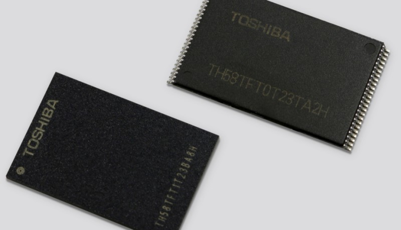
There was a time that every extra storage byte crammed into a chip was greeted with cheers and applause but today only few people will get the champagne out when an extra gigabyte or so is announced. We have become so used to the ever growing capacity of memory chips that new product launches in this area do not create much excitement anymore. Yet sometimes an event manages to stir things up a bit, like a few weeks ago when a major semiconductor manufacturer announced that it started sampling its new 32 gigabyte flash memory chip.
The manufacturer in question is Toshiba and they built the 3D Flash Memory device (as they call it) by stacking 64 layers of triple-level cells (TLCs). A TLC stocks three bits in one cell instead of one like a traditional SLC, limiting the number of cells needed to build a memory of a certain size. Because a TLC stocks eight levels (3-bit value) it takes more time to read it than a SLC and so it is a bit slower. It is also less robust.
Up to now “only” 48 layers were used, and the 16 additional layers add 40% capacity. The next milestone on the development roadmap is a 512-gigabit (64-gigabytes) device, also with 64 layers.
“Big deal, that’s just Moore’s Law, you know”, you hear some people say, “next year we will get twice as much.” Maybe we will. But a little voice inside my head keeps telling me that things are not that simple. I believe keeping up with Moore’s Law is quite an achievement.
Read full article
Hide full article
Discussion (0 comments)