
Metal ink printing for flexible electronics with self-healing capability
on
Prototype demonstrates the potential of metal ink
printing for flexible and stretchable circuits.
Researchers from North Carolina State University have developed a new technique for printing metal circuits directly, which enables flexible and stretchable electronics to be created. The technique can be applied using various metals and substrates (base materials) and is compatible with existing production systems that use direct printing methods.
"Flexible electronics is a technology with much promise, but there are considerable production costs involved to make it of practical use." says Jingyan Dong, the author of the paper and associate professor at NC State's Edward P. Fitts Department of Industrial & Systems Engineering.
Inkjet printing with metal alloys
The technique uses existing electrohydrodynamic (UHD) inkjet printing technology, which is already used in many production processes that use functional inks. Instead of ink, Dong's team uses metal alloys with melting points up to 60 degrees Celsius. The researchers have tested this technique using three different alloys on four different substrates: glass, paper and two stretchable polymers.
"This is direct printing," according to Dong. "There are no masks, etching or templates required, which makes this process much simpler".
The researchers tested the resilience of the circuits on a polymer substrate and concluded that the conductivity of the circuit was unaffected after bending 1000 times. The circuits continued to be electrically stable, even at a tensile strain of 70%.
'Self-healing' capability
The researchers also discovered that the circuits were able to “heal” themselves when they are broken or were stretched too much. "Because of the low meting point, when the affected area is heated to about 70 degrees Celsius, the metal flows towards each other and repairs the damage", says Dong.
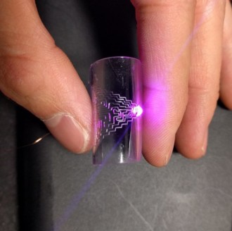
The researchers demonstrated the functionality of the printing technique by creating a high-density touch sensor and a 400-pixel array with an area of one square centimeter.
According to the researchers, the technique can be applied for the production of wearable sensors or other electronic devices.
Discussion (0 comments)