
Solar Sensor and Gateway with Display
This article describes my project for remote wireless low-power solar-powered temperature measurement device with gateway showing actual temperature from nearby sensor on display and saving it for further analysis.
This article describes my project for remote wireless low-power temperature measurement device with gateway showing actual temperature from nearby sensor on display and saving it for further analysis.
Elektor platform do not allow using images in text. All images are in attachment which you can download at the end of the article.
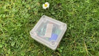
Sensor is low power small device bundled in waterproof box with transparent cover. It looks as follows. More details about sensor I will show in following sections.
IMG 01-main.jpg
Sensor is powered by small solar panel and do not have any battery. Energy harvested form sun it stores in supercapacitor. Sensor is designed for requiring no maintenance when deploys in field (for example, no battery replacement is needed). Sensor measure temperature (and supercap voltage) once per 30 seconds, and once per 15 minutes send aggregated data wirelessly using 868 MHz band. Wireless protocol is unidirectional and transmitted data are encrypted using AES encryption. Protocol I design myself as well as very compressed format of data. All these I will describe later. Board is controlled using STM32L0 MCU, but energy harvesting PMIC is very important here as well.
Gateway for receiving and saving packets received from nearby devices consists of two devices: STM32WL55 NUCLEO board which receives packets from the air, decodes (but not decrypt) them and send them over UART to STM32MP157F Discovery Board which runs OpenSTLinux and runs program (written in Rust) which decrypts packets, process them and show current values on display (GUI is implemented using GTK-rs rust library). Running gateway look as follows:
IMG 02-gateway.jpg
Now let’s see more details about hardware.
SensorFollowing picture show block diagram of the sensor device which describes hardware architecture of the device:
IMG 03-sensor-block-diagram.png
detailed is schematics which contains basically the same blocks split to multiple pages. Full schematic in PDF format as well as Kicad project is attached with the article. Device consists of following interconnected chips
It was my first sensor of this type which I designed yet. My first design work, but I did some reworks and improvements since original design. Luckily, it was possible to do all fixes without need to (significantly) rework PCB.
I will not describe all the details because of schematics, but rather I will point some interesting challenges which I faced when developing and consider them interesting.
Solar HarvesterThe most important part of design was selecting energy harvesting PMIC, solar cell and supercapacitor. Very few vendors make PMICs designed for energy harvesting and after market analysis I ended with ADP5091 which seems like most advanced one in terms of features. This may be sometimes disadvantage because for example, it requires very large resistor network for configuration. Most chips in this category (for example, BQ25570, MAX20361, EM8500, …) are very similar (and they performance and power consumption is similar). Some of them are missing some additional regulator, some of them are configured using resistors, some of them are configured over I2C, some of them has some voltage levels fixed, and so on. It was good decision, but it occupy too much space on board (PCB has 4 layers) and routing was complex. It is slightly overkill for my project, but it is very configurable.
While configuration of chip look easy at the first look it is not. There are some issues which I did not realized and since my original design and need to replace almost all configuration resistors. One issue which I did not realized is importance of start-up threshold voltage and impact of inrush currents. Harvester work in a way that it charges supercap and once it reaches certain level (referred as Power OK in case of ADP5091) it starts voltage regulator (which powers STM32L0 MCU and other parts). Once the voltage drops below different limit (referred as Stop Discharge in case of ADP5091) it turns it off. I initially set this voltage very close. I basically set Stop Discharge to minimum possible voltage (2V) and because I want to start my sensor as soon as possible I send Power OK voltage as 2.05V. The issue which I originally did not realized is that when harvester start regulator there is inrush current. Inrush current it is not clearly visible because only parts here are MCU and RF transmitter which both basically cause almost no inrush current, but there are other things connected to power rails: decoupling capacitor. When debugging cycling behaviour, I realized that once power harvester start regulator, charging decoupling caps discharges the source (supercap) below the Stop Discharge limit and harvester turn it off again. Then when regulator is off, it continues charging supercap and once it reaches Power OK voltage, pattern repeats.
The similar issue happened to me once more with different cause. Threshold voltage is not only important parameter, but supercapacitor’s internal series resistance can cause similar issues. Once the voltage regulator loads it, its voltage slightly drops which can cause stop of the voltage regulator if the voltage drops bellow configured threshold level. It can prevent circuit to boot if supercap’s ESR is too high and decoupling caps on regulated side are too large. This is one of patch which I did in my project. Originally there was only supercap, but I added 4.7uF MLCC capacitor in parallel to solve this issue.
Supercapacitor ConsiderationsOther very important parameter which I had to tune is supercapacitor. Selection of supercapacitor depends on PMIC because different PMIC have different limitations. There are three key parameters to consider: capacity, rated voltage and ESR. Importance of ESR was described in previous section. It is important but not key parameter you will choose supercap based on. The most intuitive parameter is capacity, but rated voltage is important as well and in case of some harvesting chips it is even more important. Intuitively if you charge capacitor to 2V, it will store less energy than if you charge the same capacitor to 4V. Some vendors offer supercapacitor modules consisting of two supercaps in series for increasing rated voltage but connecting capacitors in series reduces capacity (in comparison with resistors where series connection cause increase of resistance). Vendors must compensate it (by increasing capacity), so if you see 5V supercap model with capacity 1F consisting of two supercaps (rated to about 2.5V), the inner supercap are not 1F, but 2F. Basically you buy two 2F units = 4F in total and practise show that cost of these modules is about 4x higher. They offer about 4x higher energy density, but the marked capacitance is the same. When choosing if you want higher capacity or rated voltage, you need to take in account properties of your system. In my case the sensor start operating at about 2.2V, so standard supercapacitors with rated voltage 2.7V powers the circuit only in small voltage range. For this reason, I used 5.5V supercap module. But the selection always depends on requirements. Your project may have different needs than my have.
Additional impact of supercapcitor selection is start-up time. Energy harvesters do Maximum Power Point Tracking (MPPT) which cause that charging supercap by harvester behave like it is charged by constant current. Charging speed when charging by current is directly dependent on current and capacity, but not voltage. So, smaller capacitor charges faster and device with smaller capacitors (in terms of capacity) boot faster.
In my project I used 1F 5.5V dual-supercapcitor pack from Kyocera, but I tested also several other types of Cornell Dubilier's capacitor including some advanced like Lithium-Ion capacitors which combine some properties of supercapcitors like fast charge/discharge cycles and properties of Li-ion batteries like need to prevent undercharging.
OvervoltageWhen designing circuit, I learnt that with these harvesters it is good to let some margin for rated voltage. Voltage references inside harvesters are designed for low power consumption, not high accuracy. Many parts which harvester datasheet as comparators are internally implemented by digital circuit which is turned off for most time and do not check voltage continuously. For example, ADP5091 which I used most of things (like MPPT parameters) recomputes once per 16 second, but the same restriction applies for checking terminal voltage as well. If it start charging capacitor, it will charge it for full 16 second period no matter if it violate limits you set. These harvesters are designed for slow behaviours and are designed to minimize their own power consumption as much as possible.
Low Power Firmware for STM32L0Other very important part of the project is low power consumption of MCU and peripherals. It is very important to optimize it as much as possible. Higher power consumption means that you need bigger supercapacitor and at some level you will ned bigger solar panel as well. Both directly increase cost and size of the device.
Firmware utilize STOP mode and run RTC which wake up device every 30 seconds. When MCU wake up it enables and configures peripherals, measures temperature and voltage and then it goes sleep for about 30 seconds. Once per 15 minute it does additional tasks: It aggregate data, format packet, encrypt packet and transmits it. For most time the power consumption is about 1.2uA and in overall, long term power consumption is 2.2uA when voltage is lower than 3V and MCU send packet once per 15 minute. If the voltage is higher than 3V, MCU do 2 additional retransmissions for reducing data loss and these additional transmissions causes slightly higher average power consumption about 3uA. Measurements I used PPK II. I measured it using SMD jumper on board. It does not contains power consumption of harvester itself which is generally low, and there are very limited ways how to reduce it, so I consider better to measure only consumption which I can influence. Here is the screenshot from PPK showing long-term consumption from 2-minute span including transmission (last higher spike).
IMG 04-avg-consumption.png
And here is the detail of cycle which except measurement do transmission as well.
IMG 05-active-consumption.png
Phases of firmware execution are directly visible on picture. In First half regular cycle is highlighted. Two approx. 4mA spikes at beginning configures temperature sensor over i2C and triggers measurement. In the middle before third 4mA spike MCU do ADC measurements of supercapacitor voltage. This terminates before collecting temperature measurement over I2C which is third spike. As you can see this design cause that measurement and supercap voltages are measured at the same time in parallel which reduce time to do both operations and thus reduces power consumption. In case of regular cycle firmware go sleep after third 4mA spike. In case of cycle when RF transmission is needed, MCU first configure RF transmitter chip which is the long are when consumption is non-zero, but still low and then enables transmitter and start transmitting data which causes the last monumental 15mA block. At the end MCU turn off transmitter and go sleep. When MCU configures RF chip over SPI there are no spikes because SPI is push-pull bus in comparison with I2C which causes current flowing when bus is driven.
Low Power Switched High Voltage ADC MeasurementOne thing which I reworked since initial design is how I measure voltage. Supercapacitor voltage must be reduced because it is in range of 0 to 5.5V while MCU is powered by regulated 2V. Originally, I had high-value resistor voltage dividers for low power consumption. It did not work, and I learnt that ADCs do not work well with high input impedance on ADC. I fixed it by capacitor, and it looked as follows:
IMG 06-adc-div.png
It worked but still was not ideal because of permanent power consumption. I did depth analysis of 5V tolerant pins on STM32 MCUs and fond that it is possible to make switched ground on divider which will stop passing current. I reused layout of my PCB and connected resistor instead of ground to sibling pin of originally other resistor. Schematically it looks as follows.
IMG 07-5v-tol-div.png
When ADC is turned off, FT GPIO2 is in HI-Z mode, so it do not pass any current. Because current is 0, voltage drop of resistor is also 0:
U = R * I;
U = 10000 * 0
U = 0.
So, voltage on both terminals of both resistor is the same and it is supercap voltage up to about 5.5V. Now the 5V tolerant pins come in. After research in ST AN4899, I found that this is OK. 5V tolerant pin means that it accepts voltage Vcc + 3.6V. My Vcc is 2V, so maximum permitted voltage on both pins is 2 + 3.6 = 5.6V. But there is one requirement. No analog peripheral must be attached to pins. Otherwise, the 5V tolerant feature is gone and you will burn your MCU. This is important. When divider is disabled, firmware must never enable ADC. Before enabling ADC firmware bust switch FT GPIO2 from Hi-Z to Logical 0. This will make voltage on bottom terminal of R2 as 0V and resistor divider start working. On GPIO1 will be valid divided voltage, on GPIO2 will be 0V and at this moment MCU can enable ADC. After completing measurement, MCU must disable ADC first, then it can reconfigure GPIOs for disabling the divider.
Even after studying AN4899 I was not sure about correctness, so I asked on ST forum and if you are interesting on more details, you can check it here: https://community.st.com/t5/stm32-mcus-products/are-stm32l0-ft-pins-5v-tolerant-in-analog-mode-when-no-analog/td-p/608552
Packet FormatDevice send data as 20-byte frame. First 4-bytes are device id (which is computed from internal device ID provided by STM32). Next 16-bytes are one block of AES128 encrypted data. Device ID act as lookup on receiver side (gateway). AES key is embedded inf firmware and for production use you should lock your MCU. Because communication is unidirectional there are very limited options for cryptographically stronger scheme. Asymmetric cryptography is possible, but its data are much longer than 16-byte (so transmission would be much longer) and it is also more compute intensive. Both causes much higher power consumption, so I did not go this way.
Packet contains minimum, average and maximum temperatures, current supercap voltage, super cap voltage 5 minutes ago, and super cap voltage 10 minutes ago (voltage 15 minute ago was actual voltage in previous packet). Additionally, it contains header which has indication of retransmitted packed vs normal packet and also can indicate error in case of I2C or temperature sensor failure. Lastly it contains CRC. Because CRC is in encrypted data part, there very limited ways to use it for error correction, but it is still useful for determining transmission failures which due to encryption cause completely misleading data received.
Packet is transmitted using FSK encoding on 868.3 MHz band.
GatewayThe other device in the system is gateway. You need only one gateway for receiving data from multiple nearby sensors. Gateway is supposed to have stable power and is not designed as low-power device. Instead of MCU and base it on MPU. Because I had almost no requirements on gateway, I used already existing devkits instead of making my own board. I used two STM32 evaluation board for making gateway: STM32WL55 Nucleo (which I received as part of contest for free. Thank you!) and STM32MP157F Discovery which is something like Single Board Computer and in case of this board it also contains embedded display which make it very suitable for Human Machine Interface (HMI) like this one.
I considered connecting boards using Arduino connectors which are on both boards but decided to use USB connection instead. On STM32WL55 Nucleo board USB ends on ST-Link and this allows very easy Over-The-Air OTA remote updates of both devices without need for any complex work on firmware side.
STM32WL55 FirmwareSTM32WL55 send received packet as hexadecimal string over UART as well as some metadata like RSSI retrieved from integrated radio module. I used STM32CubeIDE for developing it (I used it for development of mentioned sensor’s STM32L0 firmware as well). I used code generator but cleaned generated project a lot. I like simple and clean code base. It was my first project on STM32WL55, so I have to learn a lot, but after few days I understood the architecture and it was easy to create project according my needs. Still, project has lot of code generated by STM32CubeIDE and it is useful, especially when developing more complicated Radio applications.
Gateway SoftwareSTM32MP is MPU, so it runs Linux, more precisely OpenSTLinux. This is beneficial because development look like development of standard computer program. To make it more challenging, I decide to make in Rust which I am learning now. For making GUI I used GTK library. It receives packets and do two things.
For every received packet it executes shell script, and you can do whatever you want with the packet. I log packets to file for further analysis (currently in Excel), but you can very easily call AWS or Azure CLI and send data to cloud, just by changing (or adding, if you want both CSV and cloud) single simple shell script.
For selected sensor it shows them on display. For sensors which you want to show, you need to provide AES key but gateway can forward (to cloud, for example) even packet without knowing encryption key. It will forward encrypted data and it is on your side how and where you decrypt it.
Device can show data from up to 6 sensors on screen (I currently made two prototypes of board, so on my screen, only these two sensors are shown).
I originally planned more features in this app like showing historical plots, but I am new in Rust and when I faced issues with sharing data between threads and nested GTK signal closures, I reduced my goals and currently ended up with simple and reliable application showing current data.
ConclusionThat’s all. Thank you for reading it as far. In this article I shown my two devices and firmware’s which I was working on in last months. I show my very optimized ultra-low-power solar powered battery-less sensor node with custom PCB and shown my gateway which shows data from nearby sensors on display. In article I described lot of challenges which I faced when developing this project. If you decide to make the same or similar nodes, I hope information in this article help you and hopefully, it saves you some time when you will debug your project. :)
If you are interested in more details, you see GitHub project with resources for this project: https://github.com/misaz/Elector-Contest-Solar-Sensor. It contains Kicad project for my sensor node, Schematics, firmwares for STM32L0 on sensor node and for STM32WL55 on gateway. It also contains sources of rust program which runs on gateway and process received data as well as some helper scripts which I used for building. Note that firmware for STM32L0 do not compile. You need to fill your own AES key (16 hexadecimal bytes) at the place where compiler indicate error. The same key you need to fill instead of zeroes in sample sensors.txt config on gateway side. Prebuild binary contains random key.
Elektor platform do not allow using images in text. All images are in attachment which you can download at the end of the article.
Sensor is low power small device bundled in waterproof box with transparent cover. It looks as follows. More details about sensor I will show in following sections.
IMG 01-main.jpg
Sensor is powered by small solar panel and do not have any battery. Energy harvested form sun it stores in supercapacitor. Sensor is designed for requiring no maintenance when deploys in field (for example, no battery replacement is needed). Sensor measure temperature (and supercap voltage) once per 30 seconds, and once per 15 minutes send aggregated data wirelessly using 868 MHz band. Wireless protocol is unidirectional and transmitted data are encrypted using AES encryption. Protocol I design myself as well as very compressed format of data. All these I will describe later. Board is controlled using STM32L0 MCU, but energy harvesting PMIC is very important here as well.
Gateway for receiving and saving packets received from nearby devices consists of two devices: STM32WL55 NUCLEO board which receives packets from the air, decodes (but not decrypt) them and send them over UART to STM32MP157F Discovery Board which runs OpenSTLinux and runs program (written in Rust) which decrypts packets, process them and show current values on display (GUI is implemented using GTK-rs rust library). Running gateway look as follows:
IMG 02-gateway.jpg
Now let’s see more details about hardware.
SensorFollowing picture show block diagram of the sensor device which describes hardware architecture of the device:
IMG 03-sensor-block-diagram.png
detailed is schematics which contains basically the same blocks split to multiple pages. Full schematic in PDF format as well as Kicad project is attached with the article. Device consists of following interconnected chips
- Energy Harvester PMIC (ADP5091) which harvest current-limited energy from the solar cell and charges attached supercapacitor and offers additional regulator which generates voltage for MCU, RF transmitter and temperature sensor.
- STM32L0 MCU. It is not powered for all the time. Energy harvester is powered first. After voltage on supercapacitor reaches level suitable for operation, it enables voltage regulator which powers MCU. Project utilize 5V tolerant pins of the STM32 MCU. Once MCU boot, it controls most of the circuity.
- I2C Temperature sensor has switched power (ground). Most of the time it is not powered. MCU powers it once per 30 second and then turn it off. It is connected over I2C bus to the MCU.
- RF Transmitter. Because circuit examples using STM32WL55 family are quite complicated, I chosen easier solution using external transmit-only chip. It seemed easier to implement it to me. MCU controls it over SPI. Because it is very low power and it’s power consumption is high when active, I decided to do not switch it’s power when unused.
It was my first sensor of this type which I designed yet. My first design work, but I did some reworks and improvements since original design. Luckily, it was possible to do all fixes without need to (significantly) rework PCB.
I will not describe all the details because of schematics, but rather I will point some interesting challenges which I faced when developing and consider them interesting.
Solar HarvesterThe most important part of design was selecting energy harvesting PMIC, solar cell and supercapacitor. Very few vendors make PMICs designed for energy harvesting and after market analysis I ended with ADP5091 which seems like most advanced one in terms of features. This may be sometimes disadvantage because for example, it requires very large resistor network for configuration. Most chips in this category (for example, BQ25570, MAX20361, EM8500, …) are very similar (and they performance and power consumption is similar). Some of them are missing some additional regulator, some of them are configured using resistors, some of them are configured over I2C, some of them has some voltage levels fixed, and so on. It was good decision, but it occupy too much space on board (PCB has 4 layers) and routing was complex. It is slightly overkill for my project, but it is very configurable.
While configuration of chip look easy at the first look it is not. There are some issues which I did not realized and since my original design and need to replace almost all configuration resistors. One issue which I did not realized is importance of start-up threshold voltage and impact of inrush currents. Harvester work in a way that it charges supercap and once it reaches certain level (referred as Power OK in case of ADP5091) it starts voltage regulator (which powers STM32L0 MCU and other parts). Once the voltage drops below different limit (referred as Stop Discharge in case of ADP5091) it turns it off. I initially set this voltage very close. I basically set Stop Discharge to minimum possible voltage (2V) and because I want to start my sensor as soon as possible I send Power OK voltage as 2.05V. The issue which I originally did not realized is that when harvester start regulator there is inrush current. Inrush current it is not clearly visible because only parts here are MCU and RF transmitter which both basically cause almost no inrush current, but there are other things connected to power rails: decoupling capacitor. When debugging cycling behaviour, I realized that once power harvester start regulator, charging decoupling caps discharges the source (supercap) below the Stop Discharge limit and harvester turn it off again. Then when regulator is off, it continues charging supercap and once it reaches Power OK voltage, pattern repeats.
The similar issue happened to me once more with different cause. Threshold voltage is not only important parameter, but supercapacitor’s internal series resistance can cause similar issues. Once the voltage regulator loads it, its voltage slightly drops which can cause stop of the voltage regulator if the voltage drops bellow configured threshold level. It can prevent circuit to boot if supercap’s ESR is too high and decoupling caps on regulated side are too large. This is one of patch which I did in my project. Originally there was only supercap, but I added 4.7uF MLCC capacitor in parallel to solve this issue.
Supercapacitor ConsiderationsOther very important parameter which I had to tune is supercapacitor. Selection of supercapacitor depends on PMIC because different PMIC have different limitations. There are three key parameters to consider: capacity, rated voltage and ESR. Importance of ESR was described in previous section. It is important but not key parameter you will choose supercap based on. The most intuitive parameter is capacity, but rated voltage is important as well and in case of some harvesting chips it is even more important. Intuitively if you charge capacitor to 2V, it will store less energy than if you charge the same capacitor to 4V. Some vendors offer supercapacitor modules consisting of two supercaps in series for increasing rated voltage but connecting capacitors in series reduces capacity (in comparison with resistors where series connection cause increase of resistance). Vendors must compensate it (by increasing capacity), so if you see 5V supercap model with capacity 1F consisting of two supercaps (rated to about 2.5V), the inner supercap are not 1F, but 2F. Basically you buy two 2F units = 4F in total and practise show that cost of these modules is about 4x higher. They offer about 4x higher energy density, but the marked capacitance is the same. When choosing if you want higher capacity or rated voltage, you need to take in account properties of your system. In my case the sensor start operating at about 2.2V, so standard supercapacitors with rated voltage 2.7V powers the circuit only in small voltage range. For this reason, I used 5.5V supercap module. But the selection always depends on requirements. Your project may have different needs than my have.
Additional impact of supercapcitor selection is start-up time. Energy harvesters do Maximum Power Point Tracking (MPPT) which cause that charging supercap by harvester behave like it is charged by constant current. Charging speed when charging by current is directly dependent on current and capacity, but not voltage. So, smaller capacitor charges faster and device with smaller capacitors (in terms of capacity) boot faster.
In my project I used 1F 5.5V dual-supercapcitor pack from Kyocera, but I tested also several other types of Cornell Dubilier's capacitor including some advanced like Lithium-Ion capacitors which combine some properties of supercapcitors like fast charge/discharge cycles and properties of Li-ion batteries like need to prevent undercharging.
OvervoltageWhen designing circuit, I learnt that with these harvesters it is good to let some margin for rated voltage. Voltage references inside harvesters are designed for low power consumption, not high accuracy. Many parts which harvester datasheet as comparators are internally implemented by digital circuit which is turned off for most time and do not check voltage continuously. For example, ADP5091 which I used most of things (like MPPT parameters) recomputes once per 16 second, but the same restriction applies for checking terminal voltage as well. If it start charging capacitor, it will charge it for full 16 second period no matter if it violate limits you set. These harvesters are designed for slow behaviours and are designed to minimize their own power consumption as much as possible.
Low Power Firmware for STM32L0Other very important part of the project is low power consumption of MCU and peripherals. It is very important to optimize it as much as possible. Higher power consumption means that you need bigger supercapacitor and at some level you will ned bigger solar panel as well. Both directly increase cost and size of the device.
Firmware utilize STOP mode and run RTC which wake up device every 30 seconds. When MCU wake up it enables and configures peripherals, measures temperature and voltage and then it goes sleep for about 30 seconds. Once per 15 minute it does additional tasks: It aggregate data, format packet, encrypt packet and transmits it. For most time the power consumption is about 1.2uA and in overall, long term power consumption is 2.2uA when voltage is lower than 3V and MCU send packet once per 15 minute. If the voltage is higher than 3V, MCU do 2 additional retransmissions for reducing data loss and these additional transmissions causes slightly higher average power consumption about 3uA. Measurements I used PPK II. I measured it using SMD jumper on board. It does not contains power consumption of harvester itself which is generally low, and there are very limited ways how to reduce it, so I consider better to measure only consumption which I can influence. Here is the screenshot from PPK showing long-term consumption from 2-minute span including transmission (last higher spike).
IMG 04-avg-consumption.png
And here is the detail of cycle which except measurement do transmission as well.
IMG 05-active-consumption.png
Phases of firmware execution are directly visible on picture. In First half regular cycle is highlighted. Two approx. 4mA spikes at beginning configures temperature sensor over i2C and triggers measurement. In the middle before third 4mA spike MCU do ADC measurements of supercapacitor voltage. This terminates before collecting temperature measurement over I2C which is third spike. As you can see this design cause that measurement and supercap voltages are measured at the same time in parallel which reduce time to do both operations and thus reduces power consumption. In case of regular cycle firmware go sleep after third 4mA spike. In case of cycle when RF transmission is needed, MCU first configure RF transmitter chip which is the long are when consumption is non-zero, but still low and then enables transmitter and start transmitting data which causes the last monumental 15mA block. At the end MCU turn off transmitter and go sleep. When MCU configures RF chip over SPI there are no spikes because SPI is push-pull bus in comparison with I2C which causes current flowing when bus is driven.
Low Power Switched High Voltage ADC MeasurementOne thing which I reworked since initial design is how I measure voltage. Supercapacitor voltage must be reduced because it is in range of 0 to 5.5V while MCU is powered by regulated 2V. Originally, I had high-value resistor voltage dividers for low power consumption. It did not work, and I learnt that ADCs do not work well with high input impedance on ADC. I fixed it by capacitor, and it looked as follows:
IMG 06-adc-div.png
It worked but still was not ideal because of permanent power consumption. I did depth analysis of 5V tolerant pins on STM32 MCUs and fond that it is possible to make switched ground on divider which will stop passing current. I reused layout of my PCB and connected resistor instead of ground to sibling pin of originally other resistor. Schematically it looks as follows.
IMG 07-5v-tol-div.png
When ADC is turned off, FT GPIO2 is in HI-Z mode, so it do not pass any current. Because current is 0, voltage drop of resistor is also 0:
U = R * I;
U = 10000 * 0
U = 0.
So, voltage on both terminals of both resistor is the same and it is supercap voltage up to about 5.5V. Now the 5V tolerant pins come in. After research in ST AN4899, I found that this is OK. 5V tolerant pin means that it accepts voltage Vcc + 3.6V. My Vcc is 2V, so maximum permitted voltage on both pins is 2 + 3.6 = 5.6V. But there is one requirement. No analog peripheral must be attached to pins. Otherwise, the 5V tolerant feature is gone and you will burn your MCU. This is important. When divider is disabled, firmware must never enable ADC. Before enabling ADC firmware bust switch FT GPIO2 from Hi-Z to Logical 0. This will make voltage on bottom terminal of R2 as 0V and resistor divider start working. On GPIO1 will be valid divided voltage, on GPIO2 will be 0V and at this moment MCU can enable ADC. After completing measurement, MCU must disable ADC first, then it can reconfigure GPIOs for disabling the divider.
Even after studying AN4899 I was not sure about correctness, so I asked on ST forum and if you are interesting on more details, you can check it here: https://community.st.com/t5/stm32-mcus-products/are-stm32l0-ft-pins-5v-tolerant-in-analog-mode-when-no-analog/td-p/608552
Packet FormatDevice send data as 20-byte frame. First 4-bytes are device id (which is computed from internal device ID provided by STM32). Next 16-bytes are one block of AES128 encrypted data. Device ID act as lookup on receiver side (gateway). AES key is embedded inf firmware and for production use you should lock your MCU. Because communication is unidirectional there are very limited options for cryptographically stronger scheme. Asymmetric cryptography is possible, but its data are much longer than 16-byte (so transmission would be much longer) and it is also more compute intensive. Both causes much higher power consumption, so I did not go this way.
Packet contains minimum, average and maximum temperatures, current supercap voltage, super cap voltage 5 minutes ago, and super cap voltage 10 minutes ago (voltage 15 minute ago was actual voltage in previous packet). Additionally, it contains header which has indication of retransmitted packed vs normal packet and also can indicate error in case of I2C or temperature sensor failure. Lastly it contains CRC. Because CRC is in encrypted data part, there very limited ways to use it for error correction, but it is still useful for determining transmission failures which due to encryption cause completely misleading data received.
Packet is transmitted using FSK encoding on 868.3 MHz band.
GatewayThe other device in the system is gateway. You need only one gateway for receiving data from multiple nearby sensors. Gateway is supposed to have stable power and is not designed as low-power device. Instead of MCU and base it on MPU. Because I had almost no requirements on gateway, I used already existing devkits instead of making my own board. I used two STM32 evaluation board for making gateway: STM32WL55 Nucleo (which I received as part of contest for free. Thank you!) and STM32MP157F Discovery which is something like Single Board Computer and in case of this board it also contains embedded display which make it very suitable for Human Machine Interface (HMI) like this one.
I considered connecting boards using Arduino connectors which are on both boards but decided to use USB connection instead. On STM32WL55 Nucleo board USB ends on ST-Link and this allows very easy Over-The-Air OTA remote updates of both devices without need for any complex work on firmware side.
STM32WL55 FirmwareSTM32WL55 send received packet as hexadecimal string over UART as well as some metadata like RSSI retrieved from integrated radio module. I used STM32CubeIDE for developing it (I used it for development of mentioned sensor’s STM32L0 firmware as well). I used code generator but cleaned generated project a lot. I like simple and clean code base. It was my first project on STM32WL55, so I have to learn a lot, but after few days I understood the architecture and it was easy to create project according my needs. Still, project has lot of code generated by STM32CubeIDE and it is useful, especially when developing more complicated Radio applications.
Gateway SoftwareSTM32MP is MPU, so it runs Linux, more precisely OpenSTLinux. This is beneficial because development look like development of standard computer program. To make it more challenging, I decide to make in Rust which I am learning now. For making GUI I used GTK library. It receives packets and do two things.
For every received packet it executes shell script, and you can do whatever you want with the packet. I log packets to file for further analysis (currently in Excel), but you can very easily call AWS or Azure CLI and send data to cloud, just by changing (or adding, if you want both CSV and cloud) single simple shell script.
For selected sensor it shows them on display. For sensors which you want to show, you need to provide AES key but gateway can forward (to cloud, for example) even packet without knowing encryption key. It will forward encrypted data and it is on your side how and where you decrypt it.
Device can show data from up to 6 sensors on screen (I currently made two prototypes of board, so on my screen, only these two sensors are shown).
I originally planned more features in this app like showing historical plots, but I am new in Rust and when I faced issues with sharing data between threads and nested GTK signal closures, I reduced my goals and currently ended up with simple and reliable application showing current data.
ConclusionThat’s all. Thank you for reading it as far. In this article I shown my two devices and firmware’s which I was working on in last months. I show my very optimized ultra-low-power solar powered battery-less sensor node with custom PCB and shown my gateway which shows data from nearby sensors on display. In article I described lot of challenges which I faced when developing this project. If you decide to make the same or similar nodes, I hope information in this article help you and hopefully, it saves you some time when you will debug your project. :)
If you are interested in more details, you see GitHub project with resources for this project: https://github.com/misaz/Elector-Contest-Solar-Sensor. It contains Kicad project for my sensor node, Schematics, firmwares for STM32L0 on sensor node and for STM32WL55 on gateway. It also contains sources of rust program which runs on gateway and process received data as well as some helper scripts which I used for building. Note that firmware for STM32L0 do not compile. You need to fill your own AES key (16 hexadecimal bytes) at the place where compiler indicate error. The same key you need to fill instead of zeroes in sample sensors.txt config on gateway side. Prebuild binary contains random key.
Want to build a project?
Bring your design to life with the Elektor PCB Service, powered by Eurocircuits. Upload the project files and order professionally manufactured PCBs or assembled boards through a proven European production platform.
Supporting KiCad, Eagle, Gerber, and ODB++ formats, the service is suitable for everything from prototypes and validation builds to series production and volume manufacturing.
Made in Europe. Fast. Reliable. Professional.
Discussion (0 comments)