
Surrounding-gate topology pushes Moore's law
May 30, 2018
on
on
In association with Singapore-based Unisantis Electronics the Belgian research institute Imec has developed SGTs (Surrounding Gate Transistor), a topology which enables a single SRAM cell to be fabricated using just six 5 nm transistors.
The production of smaller and smaller semiconductor structures is an ongoing goal of much of semiconductor research. As structures approach single-atom dimensions the physical limit to Moores’s Law will be reached. Using a vertical ‘Surrounding-gate’ cell topology developed by Unisantis however allows a six-transistor SRAM cell to be squeezed into an incredibly small footprint of just 0.0184 to 0.0205 μm2. A cell using this SGT topology shows a 20 to 30% reduction in area compared to SGTs using a horizontal Gate-all-around FET structure. The vertical structure also brings other advantages including improved operating voltage, stability and leakage current.
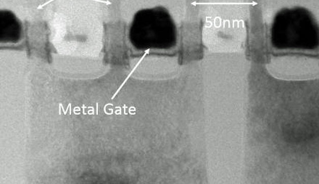
SGTs (Surroundig-Gate transistor). Image courtesy Unisantis
The use of vertical ‘surrounding-gate’ topology allows a near-perfect electrostatic control of the FET channel. An SRAM cell using this technique with a footprint of 0.0205 μm2 can be built with a minimum pillar pitch of 50 nm, resulting in a 24% better scaling factor compared to the smallest conventional SRAM cells. The manufacturing costs should be comparable to conventional finFET-based SRAMs providing the number of processes can be optimized by using single-exposure EUV lithography techniques.
The production of smaller and smaller semiconductor structures is an ongoing goal of much of semiconductor research. As structures approach single-atom dimensions the physical limit to Moores’s Law will be reached. Using a vertical ‘Surrounding-gate’ cell topology developed by Unisantis however allows a six-transistor SRAM cell to be squeezed into an incredibly small footprint of just 0.0184 to 0.0205 μm2. A cell using this SGT topology shows a 20 to 30% reduction in area compared to SGTs using a horizontal Gate-all-around FET structure. The vertical structure also brings other advantages including improved operating voltage, stability and leakage current.
The use of vertical ‘surrounding-gate’ topology allows a near-perfect electrostatic control of the FET channel. An SRAM cell using this technique with a footprint of 0.0205 μm2 can be built with a minimum pillar pitch of 50 nm, resulting in a 24% better scaling factor compared to the smallest conventional SRAM cells. The manufacturing costs should be comparable to conventional finFET-based SRAMs providing the number of processes can be optimized by using single-exposure EUV lithography techniques.
Read full article
Hide full article
Discussion (0 comments)